当前位置:
X-MOL 学术
›
Adv. Opt. Mater.
›
论文详情
Our official English website, www.x-mol.net, welcomes your
feedback! (Note: you will need to create a separate account there.)
Extending the Spectral Responsivity of MoS2 Phototransistors by Incorporating Up‐Conversion Microcrystals
Advanced Optical Materials ( IF 8.0 ) Pub Date : 2018-08-26 , DOI: 10.1002/adom.201800660 Youwei Zhang 1, 2 , Jiao Wang 1 , Bing Wang 1 , Jinhai Shao 1 , Jianan Deng 1 , Chunxiao Cong 1 , Laigui Hu 1 , Pengfei Tian 1 , Ran Liu 1 , Shi-Li Zhang 2 , Zhi-Jun Qiu 1
Advanced Optical Materials ( IF 8.0 ) Pub Date : 2018-08-26 , DOI: 10.1002/adom.201800660 Youwei Zhang 1, 2 , Jiao Wang 1 , Bing Wang 1 , Jinhai Shao 1 , Jianan Deng 1 , Chunxiao Cong 1 , Laigui Hu 1 , Pengfei Tian 1 , Ran Liu 1 , Shi-Li Zhang 2 , Zhi-Jun Qiu 1
Affiliation
|
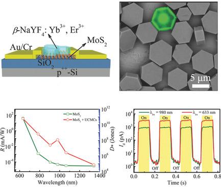
Layered 2D semiconductors are characterized by unique photoelectric properties and, therefore, constitute a new class of basic building block for next‐generation optoelectronics. However, their wide bandgaps limit the spectral responsivity to a narrow range. Here, a facile approach is demonstrated by integrating β‐NaYF4:Yb3+, Er3+ up‐conversion microcrystals (UCMCs) with monolayer‐MoS2 phototransistors to break this bandgap‐imposed barrier and to drastically extend the responsivity range. In essence, the UCMCs up‐convert a near‐infrared excitation at 980 nm to visible light of photons with energy matching the large bandgap (i.e., 1.8 eV) of monolayer‐MoS2, thereby activating the phototransistor with remarkable photocurrent and minimum interference. This approach leads to preservation of the excellent electrical merits of monolayer‐MoS2 and simultaneous retention of its low dark current and high photoresponsivity to the above‐bandgap lights. Significantly, an enhancement by over 1000 times is achieved for both responsivity and specific detectivity at 980 nm excitation. Moreover, the rate of response is kept identical to that when the MoS2 phototransistor is excited by a visible light. Therefore, integrating with UCMCs can enable the emerging 2D semiconductors of wide bandgap to respond to infrared excitations with high efficacy and without sacrificing their performance in the visible region.
中文翻译:

通过掺入上转换微晶来扩展MoS2光电晶体管的光谱响应度
分层的2D半导体具有独特的光电特性,因此构成了下一代光电子学的一类新的基本构件。但是,它们的宽带隙将光谱响应度限制在一个狭窄的范围内。在此,容易的方法是通过β-NaYF积分证实4:镱3+,铒3+上转换微晶(UCMCs)与单层-MOS 2个光电晶体管打破这种带隙强加的屏障和大幅延伸的响应范围。本质上,UCMC将980 nm处的近红外激发上转换为具有与单层MoS 2的大带隙(即1.8 eV)匹配的能量的光子可见光。,从而以显着的光电流和最小的干扰来激活光电晶体管。这种方法可以保持单层MoS 2的优异电性能,并同时保留其低暗电流和对上述带隙光的高光响应性。值得注意的是,在980 nm激发下,响应度和比检测率均提高了1000倍以上。而且,响应速率保持与当MoS 2光电晶体管被可见光激发时的响应速率相同。因此,与UCMC集成可以使宽带隙的新兴2D半导体高效响应红外激发,而不会牺牲其在可见光区域的性能。
更新日期:2018-08-26
中文翻译:
通过掺入上转换微晶来扩展MoS2光电晶体管的光谱响应度
分层的2D半导体具有独特的光电特性,因此构成了下一代光电子学的一类新的基本构件。但是,它们的宽带隙将光谱响应度限制在一个狭窄的范围内。在此,容易的方法是通过β-NaYF积分证实4:镱3+,铒3+上转换微晶(UCMCs)与单层-MOS 2个光电晶体管打破这种带隙强加的屏障和大幅延伸的响应范围。本质上,UCMC将980 nm处的近红外激发上转换为具有与单层MoS 2的大带隙(即1.8 eV)匹配的能量的光子可见光。,从而以显着的光电流和最小的干扰来激活光电晶体管。这种方法可以保持单层MoS 2的优异电性能,并同时保留其低暗电流和对上述带隙光的高光响应性。值得注意的是,在980 nm激发下,响应度和比检测率均提高了1000倍以上。而且,响应速率保持与当MoS 2光电晶体管被可见光激发时的响应速率相同。因此,与UCMC集成可以使宽带隙的新兴2D半导体高效响应红外激发,而不会牺牲其在可见光区域的性能。


 京公网安备 11010802027423号