Our official English website, www.x-mol.net, welcomes your
feedback! (Note: you will need to create a separate account there.)
Scalable faceted voids with luminescent enhanced edges in WS2 monolayers†
Nanoscale ( IF 5.8 ) Pub Date : 2018-08-08 00:00:00 , DOI: 10.1039/c8nr02246a Pawan Kumar 1, 2, 3, 4 , Dipanwita Chatterjee 4, 5, 6, 7 , Takuya Maeda 8, 9, 10, 11 , Ahin Roy 4, 5, 6, 7, 8 , Kenji Kaneko 8, 9, 10, 11 , Viswanath Balakrishnan 1, 2, 3, 4
Nanoscale ( IF 5.8 ) Pub Date : 2018-08-08 00:00:00 , DOI: 10.1039/c8nr02246a Pawan Kumar 1, 2, 3, 4 , Dipanwita Chatterjee 4, 5, 6, 7 , Takuya Maeda 8, 9, 10, 11 , Ahin Roy 4, 5, 6, 7, 8 , Kenji Kaneko 8, 9, 10, 11 , Viswanath Balakrishnan 1, 2, 3, 4
Affiliation
|
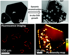
A scalable approach is needed in the formation of atomically flat edges with specific terminations to enhance local properties for optoelectronic, nanophotonic and energy applications. We demonstrate point defect clustering-driven faceted void formations with luminescent enhanced edges in WS2 monolayers during large-scale CVD growth and controlled annealing. With the aid of aberration-corrected scanning transmission electron microscopy (AC-STEM) high angle annular dark field (HAADF) imaging, we probed atomic terminations of S and W to explain observed luminescence enhancement in alternate edges. Faceted void formation in monolayer WS2 was found to be sensitive to annealing temperature, time, gas environment and precursor supply. Our observations of areal coverage evolution over time revealed competition between monolayer WS2 growth and void formation at 850 °C. While the initial stage was dominated by monolayer growth, defect generation and void growth dominated at later stages and provided an optimum processing window for monolayer WS2 as well as faceted void growth. Growth of faceted voids not only followed the geometry of monolayer facets but also showed similar atomic terminations at the edges and thus enabled local manipulation of photoluminescence enhancement with an order of magnitude increase in intensity. The developed CVD processing enabled multi-fold increase in the luminescent active edge length through the formation of faceted voids within the WS2 monolayer.
中文翻译:

WS 2单层中具有发光增强边缘的可扩展刻面空隙†
在形成具有特定端接的原子平坦边缘时,需要一种可扩展的方法来增强光电,纳米光子和能量应用的局部特性。我们证明了在大规模CVD生长和受控退火过程中,在WS 2单层中具有发光增强边缘的点缺陷聚类驱动的刻面空隙形成。借助像差校正的扫描透射电子显微镜(AC-STEM)高角度环形暗场(HAADF)成像,我们探查了S和W的原子末端,以解释在交替边缘观察到的发光增强。单层WS 2中的刻面空隙形成被发现对退火温度,时间,气体环境和前驱物供应敏感。我们观察到的随时间变化的区域覆盖范围揭示了在850°C下单层WS 2生长与空隙形成之间的竞争。初始阶段主要由单分子层生长决定,而缺陷的产生和空洞生长则在后期阶段占主导地位,并为单层WS 2提供了最佳的处理窗口以及虚空增长。刻面空隙的生长不仅遵循单层刻面的几何形状,而且在边缘处显示出相似的原子终止,因此可以对光致发光增强进行局部操作,强度增加一个数量级。通过在WS 2单层内形成多面空隙,发达的CVD处理使发光活性边缘的长度增加了许多倍。
更新日期:2018-08-08
中文翻译:
WS 2单层中具有发光增强边缘的可扩展刻面空隙†
在形成具有特定端接的原子平坦边缘时,需要一种可扩展的方法来增强光电,纳米光子和能量应用的局部特性。我们证明了在大规模CVD生长和受控退火过程中,在WS 2单层中具有发光增强边缘的点缺陷聚类驱动的刻面空隙形成。借助像差校正的扫描透射电子显微镜(AC-STEM)高角度环形暗场(HAADF)成像,我们探查了S和W的原子末端,以解释在交替边缘观察到的发光增强。单层WS 2中的刻面空隙形成被发现对退火温度,时间,气体环境和前驱物供应敏感。我们观察到的随时间变化的区域覆盖范围揭示了在850°C下单层WS 2生长与空隙形成之间的竞争。初始阶段主要由单分子层生长决定,而缺陷的产生和空洞生长则在后期阶段占主导地位,并为单层WS 2提供了最佳的处理窗口以及虚空增长。刻面空隙的生长不仅遵循单层刻面的几何形状,而且在边缘处显示出相似的原子终止,因此可以对光致发光增强进行局部操作,强度增加一个数量级。通过在WS 2单层内形成多面空隙,发达的CVD处理使发光活性边缘的长度增加了许多倍。


 京公网安备 11010802027423号