当前位置:
X-MOL 学术
›
Faraday Discuss.
›
论文详情
Our official English website, www.x-mol.net, welcomes your
feedback! (Note: you will need to create a separate account there.)
Towards a 3D GeSbTe phase change memory with integrated selector by non-aqueous electrodeposition
Faraday Discussions ( IF 3.3 ) Pub Date : 2018-07-20 , DOI: 10.1039/c8fd00126j Ruomeng Huang 1, 2, 3, 4 , Gabriela P. Kissling 2, 3, 4, 5 , Reza Kashtiban 4, 6, 7, 8 , Yasir J. Noori 1, 2, 3, 4 , Katarina Cicvarić 1, 2, 3, 4 , Wenjian Zhang 2, 3, 4, 5 , Andrew L. Hector 2, 3, 4, 5 , Richard Beanland 4, 6, 7, 8 , David C. Smith 2, 3, 4, 9 , Gillian Reid 2, 3, 4, 5 , Philip N. Bartlett 2, 3, 4, 5 , C. H. (Kees) de Groot 1, 2, 3, 4
Faraday Discussions ( IF 3.3 ) Pub Date : 2018-07-20 , DOI: 10.1039/c8fd00126j Ruomeng Huang 1, 2, 3, 4 , Gabriela P. Kissling 2, 3, 4, 5 , Reza Kashtiban 4, 6, 7, 8 , Yasir J. Noori 1, 2, 3, 4 , Katarina Cicvarić 1, 2, 3, 4 , Wenjian Zhang 2, 3, 4, 5 , Andrew L. Hector 2, 3, 4, 5 , Richard Beanland 4, 6, 7, 8 , David C. Smith 2, 3, 4, 9 , Gillian Reid 2, 3, 4, 5 , Philip N. Bartlett 2, 3, 4, 5 , C. H. (Kees) de Groot 1, 2, 3, 4
Affiliation
|
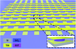
We have recently reported a new method for the electrodeposition of thin film and nanostructured phase change memory (PCM) devices from a single, highly tuneable, non-aqueous electrolyte. The quality of the material was confirmed by phase cycling via electrical pulsed switching of both 100 nm nano-cells and thin film devices. This method potentially allows deposition into extremely small confined cells down to less than 5 nm, 3D lay-outs that require non-line-of-sight techniques, and seamless integration of selector devices. As electrodeposition requires a conducting substrate, the key condition for electronic applications based on this method is the use of patterned metal lines as the working electrode during the electrodeposition process. In this paper, we show the design and fabrication of a 2D passive memory matrix in which the word lines act as the working electrode and nucleation site for the growth of confined cells of Ge–Sb–Te. We will discuss the precursor requirement for deposition from non-aqueous, weakly coordinating solvents, show the transmission electron microscopy analysis of the electrodeposition growth process and elemental distribution in the deposits, and show the fabrication and characterisation of the Ge–Sb–Te memory matrix.
中文翻译:

通过非水电沉积走向带有集成选择器的3D GeSbTe相变存储器
最近,我们已经报道了一种从单一的,高度可调节的非水电解质中电沉积薄膜和纳米结构相变存储(PCM)器件的新方法。材料的质量通过以下方式的相循环来确认100 nm纳米单元和薄膜器件的电脉冲开关。这种方法潜在地允许沉积到小于5 nm的极小密闭单元中,需要非视线技术的3D布局以及选择器设备的无缝集成。由于电沉积需要导电基板,因此基于此方法的电子应用的关键条件是在电沉积过程中使用带图案的金属线作为工作电极。在本文中,我们展示了二维被动存储矩阵的设计和制造,其中字线充当了Ge–Sb–Te受限细胞生长的工作电极和成核位点。我们将讨论从非水性弱配位溶剂中沉积的前体要求,
更新日期:2019-02-19
中文翻译:
通过非水电沉积走向带有集成选择器的3D GeSbTe相变存储器
最近,我们已经报道了一种从单一的,高度可调节的非水电解质中电沉积薄膜和纳米结构相变存储(PCM)器件的新方法。材料的质量通过以下方式的相循环来确认100 nm纳米单元和薄膜器件的电脉冲开关。这种方法潜在地允许沉积到小于5 nm的极小密闭单元中,需要非视线技术的3D布局以及选择器设备的无缝集成。由于电沉积需要导电基板,因此基于此方法的电子应用的关键条件是在电沉积过程中使用带图案的金属线作为工作电极。在本文中,我们展示了二维被动存储矩阵的设计和制造,其中字线充当了Ge–Sb–Te受限细胞生长的工作电极和成核位点。我们将讨论从非水性弱配位溶剂中沉积的前体要求,


 京公网安备 11010802027423号