当前位置:
X-MOL 学术
›
Chem. Soc. Rev.
›
论文详情
Our official English website, www.x-mol.net, welcomes your
feedback! (Note: you will need to create a separate account there.)
Emerging photonic architectures in two-dimensional opto-electronics
Chemical Society Reviews ( IF 40.4 ) Pub Date : 2018-07-19 00:00:00 , DOI: 10.1039/c8cs00206a Victor W. Brar 1, 2, 3, 4 , Michelle C. Sherrott 4, 5, 6, 7 , Deep Jariwala 4, 8, 9, 10
Chemical Society Reviews ( IF 40.4 ) Pub Date : 2018-07-19 00:00:00 , DOI: 10.1039/c8cs00206a Victor W. Brar 1, 2, 3, 4 , Michelle C. Sherrott 4, 5, 6, 7 , Deep Jariwala 4, 8, 9, 10
Affiliation
|
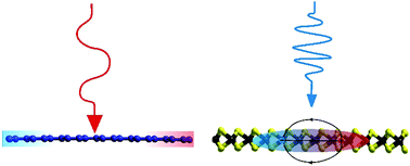
The isolation of thermodynamically stable, free standing materials with single to few atom thicknesses has brought about a revolution in materials science, condensed matter physics and device engineering for opto-electronic applications. These two dimensional (2D) materials cover a broad range of electronic properties ranging from zero-band gap, semi-metallic graphene to wide band gap semiconductors in sulfides and selenides of Mo and W to metallic behavior in Ti, Nb and Ta sulfides and selenides. This permits their potential application in opto-electronic devices from terahertz frequencies up to the ultraviolet portion of the spectrum. However, their atomically thin nature poses fundamental challenges in driving efficient light–matter interactions. A range of strategies have been explored from the area of photonics and resonant optics that enhance the coupling and interaction of light with atomically thin layers to overcome this challenge. By comparing and contrasting critical advantages of integrating nanophotonic elements with 2D materials, this review highlights the challenges and advantages of such opto-electronic devices.
中文翻译:

二维光电中的新兴光子架构
具有单个或几个原子厚度的热力学稳定的独立式材料的隔离引发了材料科学,凝聚态物理和光电应用设备工程领域的一场革命。这两种二维(2D)材料涵盖了广泛的电子特性,从零带隙,半金属石墨烯到Mo和W的硫化物和硒化物中的宽带隙半导体,到Ti,Nb和Ta的硫化物和硒化物中的金属行为。 。这使得它们有可能在太赫兹频率到光谱的紫外线部分的光电设备中应用。但是,它们的原子稀薄性质对驱动有效的光-物质相互作用提出了根本性的挑战。已经从光子学和共振光学领域探索了一系列策略,这些策略增强了光与原子薄层的耦合和相互作用,从而克服了这一挑战。通过比较和对比将纳米光子元件与2D材料集成在一起的关键优势,本文重点介绍了此类光电设备的挑战和优势。
更新日期:2018-07-19
中文翻译:
二维光电中的新兴光子架构
具有单个或几个原子厚度的热力学稳定的独立式材料的隔离引发了材料科学,凝聚态物理和光电应用设备工程领域的一场革命。这两种二维(2D)材料涵盖了广泛的电子特性,从零带隙,半金属石墨烯到Mo和W的硫化物和硒化物中的宽带隙半导体,到Ti,Nb和Ta的硫化物和硒化物中的金属行为。 。这使得它们有可能在太赫兹频率到光谱的紫外线部分的光电设备中应用。但是,它们的原子稀薄性质对驱动有效的光-物质相互作用提出了根本性的挑战。已经从光子学和共振光学领域探索了一系列策略,这些策略增强了光与原子薄层的耦合和相互作用,从而克服了这一挑战。通过比较和对比将纳米光子元件与2D材料集成在一起的关键优势,本文重点介绍了此类光电设备的挑战和优势。


 京公网安备 11010802027423号