Our official English website, www.x-mol.net, welcomes your
feedback! (Note: you will need to create a separate account there.)
Electron ptychography of 2D materials to deep sub-ångström resolution
Nature ( IF 50.5 ) Pub Date : 2018-07-01 , DOI: 10.1038/s41586-018-0298-5 Yi Jiang , Zhen Chen , Yimo Han , Pratiti Deb , Hui Gao , Saien Xie , Prafull Purohit , Mark W. Tate , Jiwoong Park , Sol M. Gruner , Veit Elser , David A. Muller
Nature ( IF 50.5 ) Pub Date : 2018-07-01 , DOI: 10.1038/s41586-018-0298-5 Yi Jiang , Zhen Chen , Yimo Han , Pratiti Deb , Hui Gao , Saien Xie , Prafull Purohit , Mark W. Tate , Jiwoong Park , Sol M. Gruner , Veit Elser , David A. Muller
|
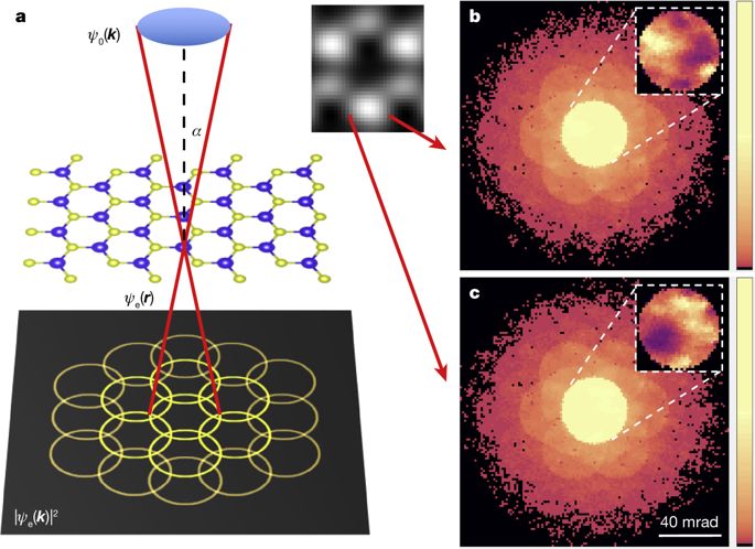
Aberration-corrected optics have made electron microscopy at atomic resolution a widespread and often essential tool for characterizing nanoscale structures. Image resolution has traditionally been improved by increasing the numerical aperture of the lens (α) and the beam energy, with the state-of-the-art at 300 kiloelectronvolts just entering the deep sub-ångström (that is, less than 0.5 ångström) regime. Two-dimensional (2D) materials are imaged at lower beam energies to avoid displacement damage from large momenta transfers, limiting spatial resolution to about 1 ångström. Here, by combining an electron microscope pixel-array detector with the dynamic range necessary to record the complete distribution of transmitted electrons and full-field ptychography to recover phase information from the full phase space, we increase the spatial resolution well beyond the traditional numerical-aperture-limited resolution. At a beam energy of 80 kiloelectronvolts, our ptychographic reconstruction improves the image contrast of single-atom defects in MoS2 substantially, reaching an information limit close to 5α, which corresponds to an Abbe diffraction-limited resolution of 0.39 ångström, at the electron dose and imaging conditions for which conventional imaging methods reach only 0.98 ångström.Combining an electron microscope pixel-array detector that collects the entire distribution of scattered electrons with full-field ptychography greatly improves image resolution and contrast compared to traditional techniques, even at low beam energies.
中文翻译:

2D 材料的电子 ptychography 至深亚 ngström 分辨率
像差校正光学已经使原子分辨率的电子显微镜成为表征纳米级结构的广泛且通常必不可少的工具。传统上通过增加透镜的数值孔径 (α) 和光束能量来提高图像分辨率,最先进的 300 千电子伏特刚刚进入深亚 ångström(即小于 0.5 ångström)政权。二维 (2D) 材料在较低的光束能量下成像,以避免大动量传递造成的位移损坏,将空间分辨率限制在约 1 ångström。在这里,通过将电子显微镜像素阵列探测器与记录透射电子的完整分布和全场 ptychography 所需的动态范围相结合,从全相空间中恢复相位信息,我们将空间分辨率提高到远远超过传统的数值孔径限制分辨率。在 80 千电子伏特的束能量下,我们的 ptychographic 重建显着提高了 MoS2 中单原子缺陷的图像对比度,达到接近 5α 的信息极限,这对应于 0.39 ångström 的阿贝衍射极限分辨率,在电子剂量和传统成像方法仅达到 0.98 ångström 的成像条件。 与传统技术相比,即使在低光束能量下,将收集整个散射电子分布的电子显微镜像素阵列探测器与全场 ptychography 相结合,也大大提高了图像分辨率和对比度。
更新日期:2018-07-01
中文翻译:
2D 材料的电子 ptychography 至深亚 ngström 分辨率
像差校正光学已经使原子分辨率的电子显微镜成为表征纳米级结构的广泛且通常必不可少的工具。传统上通过增加透镜的数值孔径 (α) 和光束能量来提高图像分辨率,最先进的 300 千电子伏特刚刚进入深亚 ångström(即小于 0.5 ångström)政权。二维 (2D) 材料在较低的光束能量下成像,以避免大动量传递造成的位移损坏,将空间分辨率限制在约 1 ångström。在这里,通过将电子显微镜像素阵列探测器与记录透射电子的完整分布和全场 ptychography 所需的动态范围相结合,从全相空间中恢复相位信息,我们将空间分辨率提高到远远超过传统的数值孔径限制分辨率。在 80 千电子伏特的束能量下,我们的 ptychographic 重建显着提高了 MoS2 中单原子缺陷的图像对比度,达到接近 5α 的信息极限,这对应于 0.39 ångström 的阿贝衍射极限分辨率,在电子剂量和传统成像方法仅达到 0.98 ångström 的成像条件。 与传统技术相比,即使在低光束能量下,将收集整个散射电子分布的电子显微镜像素阵列探测器与全场 ptychography 相结合,也大大提高了图像分辨率和对比度。


 京公网安备 11010802027423号