当前位置:
X-MOL 学术
›
Adv. Electron. Mater.
›
论文详情
Our official English website, www.x-mol.net, welcomes your
feedback! (Note: you will need to create a separate account there.)
High Detectivity from a Lateral Graphene–MoS2 Schottky Photodetector Grown by Chemical Vapor Deposition
Advanced Electronic Materials ( IF 5.3 ) Pub Date : 2018-07-16 , DOI: 10.1002/aelm.201800069 Wenjie Deng 1 , Yongfeng Chen 1 , Congya You 1 , Beiyun Liu 1 , Yanhan Yang 1 , Gaoliang Shen 1 , Songyu Li 1 , Ling Sun 2 , Yongzhe Zhang 1 , Hui Yan 1
Advanced Electronic Materials ( IF 5.3 ) Pub Date : 2018-07-16 , DOI: 10.1002/aelm.201800069 Wenjie Deng 1 , Yongfeng Chen 1 , Congya You 1 , Beiyun Liu 1 , Yanhan Yang 1 , Gaoliang Shen 1 , Songyu Li 1 , Ling Sun 2 , Yongzhe Zhang 1 , Hui Yan 1
Affiliation
|
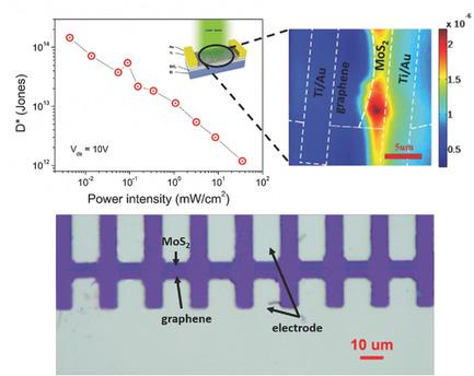
2D material–based photodetectors have demonstrated the great potential in future optoelectric applications and the compatibility with the traditional semiconductor technology. However, low detectivity and difficulty of large‐scale fabrication still limit their application. Here, an ultrasensitive in‐plane lateral graphene–MoS2 heterostructure is successfully constructed using one‐step growth by chemical vapor deposition, which is suitable for large‐scale fabrication. The Schottky junction is formed in the channel with the edge contact of graphene and MoS2. It displays good rectification characteristics with an on/off ratio up to 106. As a photodetector, it exhibits excellent detectivity with the specific detectivity D* up to 1.4 × 10¹⁴ Jones and the responsivity of 1.1 × 10⁵ A W−1, which benefit from strong absorption, the efficient separation of the photoexcited carriers, and quick charge transport in the Schottky junction device. Moreover, heterostructure photodetector array is demonstrated here which shows the large‐scale fabrication capacity. All of these results prove the potential of 2D material–based junction devices for optoelectronic devices.
中文翻译:

化学气相沉积生长的横向石墨烯-MoS2肖特基光电探测器的高检测灵敏度
基于2D材料的光电探测器已经证明了其在未来光电应用中的巨大潜力以及与传统半导体技术的兼容性。但是,低探测性和大规模制造的困难仍然限制了它们的应用。在这里,通过化学气相沉积一步生长成功地构建了超灵敏的平面侧向石墨烯-MoS 2异质结构,适用于大规模制造。肖特基结与石墨烯和MoS 2的边缘接触在沟道中形成。它显示出良好的整流特性,开/关比最高为10 6。作为光电检测器,它具有出色的检测能力,比检测能力D *高达1.4×10¹⁴琼斯和1.1×10 5 AW -1的响应度,受益于强吸收,有效分离光激发载流子以及肖特基结器件中的快速电荷传输。此外,这里展示了异质结构光电探测器阵列,显示了大规模的制造能力。所有这些结果证明了基于2D材料的结器件在光电器件中的潜力。
更新日期:2018-07-16
中文翻译:
化学气相沉积生长的横向石墨烯-MoS2肖特基光电探测器的高检测灵敏度
基于2D材料的光电探测器已经证明了其在未来光电应用中的巨大潜力以及与传统半导体技术的兼容性。但是,低探测性和大规模制造的困难仍然限制了它们的应用。在这里,通过化学气相沉积一步生长成功地构建了超灵敏的平面侧向石墨烯-MoS 2异质结构,适用于大规模制造。肖特基结与石墨烯和MoS 2的边缘接触在沟道中形成。它显示出良好的整流特性,开/关比最高为10 6。作为光电检测器,它具有出色的检测能力,比检测能力D *高达1.4×10¹⁴琼斯和1.1×10 5 AW -1的响应度,受益于强吸收,有效分离光激发载流子以及肖特基结器件中的快速电荷传输。此外,这里展示了异质结构光电探测器阵列,显示了大规模的制造能力。所有这些结果证明了基于2D材料的结器件在光电器件中的潜力。


 京公网安备 11010802027423号