Nano Research ( IF 9.5 ) Pub Date : 2018-07-14 , DOI: 10.1007/s12274-018-2141-6 Ondrej Dyck , Songkil Kim , Sergei V. Kalinin , Stephen Jesse
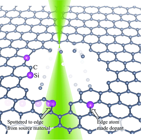
The burgeoning field of atomic-level material control holds great promise for future breakthroughs in quantum and memristive device manufacture and fundamental studies of atomic-scale chemistry. Realization of atom-by-atom control of matter represents a complex and ongoing challenge. Here, we explore the feasibility of controllable motion of dopant Si atoms at the edges of graphene via the sub-atomically focused electron beam in a scanning transmission electron microscope. We demonstrate that the graphene edges can be cleaned of Si atoms and then subsequently replenished from nearby source material. It is also shown how Si edge atoms may be “pushed” from the edge of a small hole into the bulk of the graphene lattice and from the bulk of the lattice back to the edge. This is accomplished through sputtering of the edge of the graphene lattice to bury or uncover Si dopant atoms. Finally, we demonstrate e-beam mediated hole healing and incorporation of dopant atoms. These experiments form an initial step toward general atomic-scale material control.
中文翻译:
像差校正扫描透射电子显微镜对石墨烯边缘的Si原子进行电子束处理
原子级材料控制的新兴领域为量子和忆阻器件制造以及原子级化学基础研究的未来突破提供了广阔的前景。物质的逐个原子控制的实现是一个复杂而持续的挑战。在这里,我们通过扫描透射电子显微镜中的亚原子聚焦电子束,探索了石墨烯边缘的掺杂剂Si原子可控运动的可行性。我们证明,石墨烯边缘可以清除Si原子,然后从附近的源材料中补充。还显示了如何将Si边缘原子从一个小孔的边缘“推入”到石墨烯晶格的大部分中,以及从晶格的大部分返回到边缘。这是通过溅射石墨烯晶格的边缘以掩埋或发现Si掺杂剂原子来实现的。最后,我们证明了电子束介导的空穴愈合和掺杂原子的结合。这些实验形成了向一般原子级材料控制迈出的第一步。


 京公网安备 11010802027423号