当前位置:
X-MOL 学术
›
Adv. Mater. Interfaces
›
论文详情
Our official English website, www.x-mol.net, welcomes your
feedback! (Note: you will need to create a separate account there.)
Plasma‐Etched Nanosphere Conductivity‐Inverted Lithography (PENCIL): A Facile Fabrication of Size‐Tunable Gold Disc Array on ITO‐Coated Glass
Advanced Materials Interfaces ( IF 4.3 ) Pub Date : 2018-07-11 , DOI: 10.1002/admi.201800477 Aroonsri Ngamaroonchote 1 , Tanyakorn Muangnapoh 1 , Noppadol Aroonyadet 1 , Pisist Kumnorkaew 1 , Rawiwan Laocharoensuk 1
Advanced Materials Interfaces ( IF 4.3 ) Pub Date : 2018-07-11 , DOI: 10.1002/admi.201800477 Aroonsri Ngamaroonchote 1 , Tanyakorn Muangnapoh 1 , Noppadol Aroonyadet 1 , Pisist Kumnorkaew 1 , Rawiwan Laocharoensuk 1
Affiliation
|
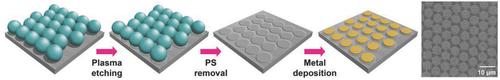
Nanosphere lithography is employed to simply fabricate metallic hexagonal nanohole array based on metal deposition within interstices of the nanospheres. In contrast, fabrication of nanodisc array (inverted pattern of nanohole array) unavoidably includes an additional step of creating a patterned resist layer or the use of high‐resolution lithography techniques. In this work, a facile method named “plasma‐etched nanosphere conductivity‐inverted lithography (PENCIL)” is developed to fabricate gold disc arrays on indium tin oxide (ITO)‐coated glass by simply incorporating plasma etching of nanosphere lithographic mask and electrodeposition of metal. The hexagonal close‐packed polystyrene (PS) spheres are served as mask for blocking an interaction of oxygen plasma and ITO surface. Topographic images and current mappings reveal different thicknesses and conductivities of plasma‐etched ITO surface. The exposed surface (gap area) exhibits higher resistivity compare with the area protected by spheres. As a result, site‐selective electrodeposition of gold is produced on patterned substrate. The microdiscs size, as well as the size and density of nanoparticles situated within the disc area can be tuned via etching and electrodeposition conditions. This suggests a simple, low‐cost, and high‐throughput technique, which potentially facilitate the expansive use of metal disc array in studying the structural dependent properties of nanomaterials.
中文翻译:

等离子刻蚀纳米球电导率反向光刻技术(PENCIL):在ITO涂层玻璃上方便地制作尺寸可调的金盘阵列
基于纳米球间隙中的金属沉积,采用纳米球光刻技术来简单地制造金属六边形纳米孔阵列。相反,纳米盘阵列(纳米孔阵列的倒置图案)的制造不可避免地包括创建图案化抗蚀剂层或使用高分辨率光刻技术的附加步骤。在这项工作中,开发了一种名为“等离子刻蚀纳米球电导率倒置光刻法(PENCIL)”的简便方法,该方法通过简单地将纳米球刻蚀掩模的等离子刻蚀和电沉积工艺结合在一起,从而在氧化铟锡(ITO)涂层的玻璃上制作金盘阵列。金属。六角形紧密堆积的聚苯乙烯(PS)球用作遮罩,以阻止氧等离子体与ITO表面的相互作用。地形图和电流图显示了等离子刻蚀的ITO表面的不同厚度和电导率。与球体保护的区域相比,裸露的表面(间隙区域)显示出更高的电阻率。结果,在有图案的基材上产生了金的位置选择电沉积。可以通过蚀刻和电沉积条件来调整微光盘的大小,以及位于光盘区域内的纳米粒子的大小和密度。这表明了一种简单,低成本和高通量的技术,它有可能促进金属圆盘阵列在研究纳米材料的结构相关特性方面的广泛使用。在有图案的基材上产生金的定点电沉积。可以通过蚀刻和电沉积条件来调整微光盘的大小,以及位于光盘区域内的纳米粒子的大小和密度。这表明了一种简单,低成本和高通量的技术,它有可能促进金属圆盘阵列在研究纳米材料的结构相关特性方面的广泛使用。在有图案的基材上产生金的定点电沉积。可以通过蚀刻和电沉积条件来调整微光盘的大小,以及位于光盘区域内的纳米粒子的大小和密度。这表明了一种简单,低成本和高通量的技术,它有可能促进金属圆盘阵列在研究纳米材料的结构相关特性方面的广泛使用。
更新日期:2018-07-11
中文翻译:
等离子刻蚀纳米球电导率反向光刻技术(PENCIL):在ITO涂层玻璃上方便地制作尺寸可调的金盘阵列
基于纳米球间隙中的金属沉积,采用纳米球光刻技术来简单地制造金属六边形纳米孔阵列。相反,纳米盘阵列(纳米孔阵列的倒置图案)的制造不可避免地包括创建图案化抗蚀剂层或使用高分辨率光刻技术的附加步骤。在这项工作中,开发了一种名为“等离子刻蚀纳米球电导率倒置光刻法(PENCIL)”的简便方法,该方法通过简单地将纳米球刻蚀掩模的等离子刻蚀和电沉积工艺结合在一起,从而在氧化铟锡(ITO)涂层的玻璃上制作金盘阵列。金属。六角形紧密堆积的聚苯乙烯(PS)球用作遮罩,以阻止氧等离子体与ITO表面的相互作用。地形图和电流图显示了等离子刻蚀的ITO表面的不同厚度和电导率。与球体保护的区域相比,裸露的表面(间隙区域)显示出更高的电阻率。结果,在有图案的基材上产生了金的位置选择电沉积。可以通过蚀刻和电沉积条件来调整微光盘的大小,以及位于光盘区域内的纳米粒子的大小和密度。这表明了一种简单,低成本和高通量的技术,它有可能促进金属圆盘阵列在研究纳米材料的结构相关特性方面的广泛使用。在有图案的基材上产生金的定点电沉积。可以通过蚀刻和电沉积条件来调整微光盘的大小,以及位于光盘区域内的纳米粒子的大小和密度。这表明了一种简单,低成本和高通量的技术,它有可能促进金属圆盘阵列在研究纳米材料的结构相关特性方面的广泛使用。在有图案的基材上产生金的定点电沉积。可以通过蚀刻和电沉积条件来调整微光盘的大小,以及位于光盘区域内的纳米粒子的大小和密度。这表明了一种简单,低成本和高通量的技术,它有可能促进金属圆盘阵列在研究纳米材料的结构相关特性方面的广泛使用。


 京公网安备 11010802027423号