当前位置:
X-MOL 学术
›
J. Am. Chem. Soc.
›
论文详情
Our official English website, www.x-mol.net, welcomes your
feedback! (Note: you will need to create a separate account there.)
Super-Resolution Imaging of Clickable Graphene Nanoribbons Decorated with Fluorescent Dyes
Journal of the American Chemical Society ( IF 14.4 ) Pub Date : 2018-07-05 , DOI: 10.1021/jacs.8b04679 Dharati Joshi 1 , Meghan Hauser 1 , Gregory Veber 1 , Alexandra Berl 1 , Ke Xu 1, 2 , Felix R. Fischer 1, 3, 4
Journal of the American Chemical Society ( IF 14.4 ) Pub Date : 2018-07-05 , DOI: 10.1021/jacs.8b04679 Dharati Joshi 1 , Meghan Hauser 1 , Gregory Veber 1 , Alexandra Berl 1 , Ke Xu 1, 2 , Felix R. Fischer 1, 3, 4
Affiliation
|
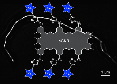
The functional integration of atomically defined graphene nanoribbons (GNRs) into single-ribbon electronic device architectures has been limited by access to nondestructive high-resolution imaging techniques that are both compatible with common supports such as Si or Si/SiO2 wafers and capable of resolving individual ribbons in dilute samples. Conventional techniques such as scanning probe (AFM, STM) or electron microscopy (SEM, TEM) have been restricted by requisite sample preparation techniques that are incompatible with lithographic device fabrication. Here we report the design and synthesis of ultralong (∼10 μm) cove-type GNRs (cGNRs) featuring azide groups along the edges that can serve as a universal handle for late-stage functionalization with terminal alkynes. Copper-catalyzed click-chemistry with Cy5 fluorescent dyes gives rise to cGNRs decorated along the edges with fluorescent tags detectable by optical microscopy. The structures of individual dye-functionalized cGNRs spin-coated from a dilute solution onto transparent and opaque insulating substrates were resolved using diffraction-limited fluorescence microscopy and super-resolution microscopy (SRM) imaging techniques. Analysis of SRM images reveals an apparent width of cGNRs in the range 40-50 nm and lengths in excess of 10 μm, the longest GNRs imaged to date. Isolated cGNRs can even be distinguished from bundles and larger aggregates as long as the center-to-center distance is greater than the apparent width.
中文翻译:

荧光染料装饰的可点击石墨烯纳米带的超分辨率成像
原子定义的石墨烯纳米带 (GNR) 与单带电子器件架构的功能集成受到非破坏性高分辨率成像技术的限制,这些技术既与 Si 或 Si/SiO2 晶片等常见载体兼容,又能够解析单个稀释样品中的色带。扫描探针(AFM、STM)或电子显微镜(SEM、TEM)等传统技术受到与光刻设备制造不兼容的必要样品制备技术的限制。在这里,我们报告了超长(~10 μm)凹形 GNR(cGNR)的设计和合成,其边缘具有叠氮化物基团,可作为末端炔烃后期功能化的通用手柄。铜催化的点击化学与 Cy5 荧光染料产生了沿边缘装饰的 cGNR,荧光标记可通过光学显微镜检测到。使用衍射极限荧光显微镜和超分辨率显微镜 (SRM) 成像技术解析了从稀溶液旋涂到透明和不透明绝缘基板上的单个染料功能化 cGNR 的结构。SRM 图像分析显示 cGNR 的表观宽度在 40-50 nm 范围内,长度超过 10 μm,这是迄今为止成像的最长 GNR。只要中心到中心的距离大于表观宽度,孤立的 cGNR 甚至可以与束和更大的聚集体区分开来。使用衍射极限荧光显微镜和超分辨率显微镜 (SRM) 成像技术解析了从稀溶液旋涂到透明和不透明绝缘基板上的单个染料功能化 cGNR 的结构。SRM 图像分析显示 cGNR 的表观宽度在 40-50 nm 范围内,长度超过 10 μm,这是迄今为止成像的最长 GNR。只要中心到中心的距离大于表观宽度,孤立的 cGNR 甚至可以与束和更大的聚集体区分开来。使用衍射极限荧光显微镜和超分辨率显微镜 (SRM) 成像技术解析了从稀溶液旋涂到透明和不透明绝缘基板上的单个染料功能化 cGNR 的结构。SRM 图像分析显示 cGNR 的表观宽度在 40-50 nm 范围内,长度超过 10 μm,这是迄今为止成像的最长 GNR。只要中心到中心的距离大于表观宽度,孤立的 cGNR 甚至可以与束和更大的聚集体区分开来。SRM 图像分析显示 cGNR 的表观宽度在 40-50 nm 范围内,长度超过 10 μm,这是迄今为止成像的最长 GNR。只要中心到中心的距离大于表观宽度,孤立的 cGNR 甚至可以与束和更大的聚集体区分开来。SRM 图像分析显示 cGNR 的表观宽度在 40-50 nm 范围内,长度超过 10 μm,这是迄今为止成像的最长 GNR。只要中心到中心的距离大于表观宽度,孤立的 cGNR 甚至可以与束和更大的聚集体区分开来。
更新日期:2018-07-05
中文翻译:
荧光染料装饰的可点击石墨烯纳米带的超分辨率成像
原子定义的石墨烯纳米带 (GNR) 与单带电子器件架构的功能集成受到非破坏性高分辨率成像技术的限制,这些技术既与 Si 或 Si/SiO2 晶片等常见载体兼容,又能够解析单个稀释样品中的色带。扫描探针(AFM、STM)或电子显微镜(SEM、TEM)等传统技术受到与光刻设备制造不兼容的必要样品制备技术的限制。在这里,我们报告了超长(~10 μm)凹形 GNR(cGNR)的设计和合成,其边缘具有叠氮化物基团,可作为末端炔烃后期功能化的通用手柄。铜催化的点击化学与 Cy5 荧光染料产生了沿边缘装饰的 cGNR,荧光标记可通过光学显微镜检测到。使用衍射极限荧光显微镜和超分辨率显微镜 (SRM) 成像技术解析了从稀溶液旋涂到透明和不透明绝缘基板上的单个染料功能化 cGNR 的结构。SRM 图像分析显示 cGNR 的表观宽度在 40-50 nm 范围内,长度超过 10 μm,这是迄今为止成像的最长 GNR。只要中心到中心的距离大于表观宽度,孤立的 cGNR 甚至可以与束和更大的聚集体区分开来。使用衍射极限荧光显微镜和超分辨率显微镜 (SRM) 成像技术解析了从稀溶液旋涂到透明和不透明绝缘基板上的单个染料功能化 cGNR 的结构。SRM 图像分析显示 cGNR 的表观宽度在 40-50 nm 范围内,长度超过 10 μm,这是迄今为止成像的最长 GNR。只要中心到中心的距离大于表观宽度,孤立的 cGNR 甚至可以与束和更大的聚集体区分开来。使用衍射极限荧光显微镜和超分辨率显微镜 (SRM) 成像技术解析了从稀溶液旋涂到透明和不透明绝缘基板上的单个染料功能化 cGNR 的结构。SRM 图像分析显示 cGNR 的表观宽度在 40-50 nm 范围内,长度超过 10 μm,这是迄今为止成像的最长 GNR。只要中心到中心的距离大于表观宽度,孤立的 cGNR 甚至可以与束和更大的聚集体区分开来。SRM 图像分析显示 cGNR 的表观宽度在 40-50 nm 范围内,长度超过 10 μm,这是迄今为止成像的最长 GNR。只要中心到中心的距离大于表观宽度,孤立的 cGNR 甚至可以与束和更大的聚集体区分开来。SRM 图像分析显示 cGNR 的表观宽度在 40-50 nm 范围内,长度超过 10 μm,这是迄今为止成像的最长 GNR。只要中心到中心的距离大于表观宽度,孤立的 cGNR 甚至可以与束和更大的聚集体区分开来。


 京公网安备 11010802027423号