当前位置:
X-MOL 学术
›
J. Am. Chem. Soc.
›
论文详情
Our official English website, www.x-mol.net, welcomes your feedback! (Note: you will need to create a separate account there.)
Defect Engineering for High Performance N-type PbSe Thermoelectrics
Journal of the American Chemical Society ( IF 15.0 ) Pub Date : 2018-06-29 , DOI: 10.1021/jacs.8b05741 Chongjian Zhou 1 , Yong Kyu Lee 1 , Joonil Cha 1 , Byeongjun Yoo 1 , Sung-Pyo Cho , Taeghwan Hyeon 1 , In Chung 1
Journal of the American Chemical Society ( IF 15.0 ) Pub Date : 2018-06-29 , DOI: 10.1021/jacs.8b05741 Chongjian Zhou 1 , Yong Kyu Lee 1 , Joonil Cha 1 , Byeongjun Yoo 1 , Sung-Pyo Cho , Taeghwan Hyeon 1 , In Chung 1
Affiliation
|
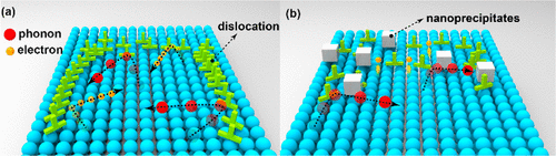
Introducing structural defects such as vacancies, nanoprecipitates, and dislocations is a proven means of reducing lattice thermal conductivity. However, these defects tend to be detrimental to carrier mobility. Consequently, the overall effects for enhancing ZT are often compromised. Indeed, developing strategies allowing for strong phonon scattering and high carrier mobility at the same time is a prime task in thermoelectrics. Here we present a high-performance thermoelectric system of Pb0.95(Sb0.033□0.017)Se1- yTe y (□ = vacancy; y = 0-0.4) embedded with unique defect architecture. Given the mean free paths of phonons and electrons, we rationally integrate multiple defects that involve point defects, vacancy-driven dense dislocations, and Te-induced nanoprecipitates with different sizes and mass fluctuations. They collectively scatter thermal phonons in a wide range of frequencies to give lattice thermal conductivity of ∼0.4 W m-1 K-1, which approaches to the amorphous limit. Remarkably, Te alloying increases a density of nanoprecipitates that affect mobility negligibly and impede phonons significantly, and it also decreases a density of dislocations that scatter both electrons and phonons heavily. As y is increased to 0.4, electron mobility is enhanced and lattice thermal conductivity is decreased simultaneously. As a result, Pb0.95(Sb0.033□0.017)Se0.6Te0.4 exhibits the highest ZT ∼ 1.5 at 823 K, which is attributed to the markedly enhanced power factor and reduced lattice thermal conductivity, in comparison with a ZT ∼ 0.9 for Pb0.95(Sb0.033□0.017)Se that contains heavy dislocations only. These results highlight the potential of defect engineering to modulate electrical and thermal transport properties independently. We also reveal the defect formation mechanisms for dislocations and nanoprecipitates embedded in Pb0.95(Sb0.033□0.017)Se0.6Te0.4 by atomic resolution spherical aberration-corrected scanning transmission electron microscopy.
中文翻译:

高性能 N 型 PbSe 热电器件的缺陷工程
引入结构缺陷,如空位、纳米沉淀和位错,是降低晶格热导率的一种行之有效的方法。然而,这些缺陷往往不利于载流子迁移率。因此,增强 ZT 的整体效果通常会受到影响。事实上,开发同时允许强声子散射和高载流子迁移率的策略是热电学的主要任务。在这里,我们提出了一种嵌入独特缺陷结构的 Pb0.95(Sb0.033□0.017)Se1-yTe y(□ = 空位;y = 0-0.4)的高性能热电系统。鉴于声子和电子的平均自由程,我们合理地整合了多个缺陷,包括点缺陷、空位驱动的致密位错和不同尺寸和质量波动的 Te 诱导纳米沉淀。它们在很宽的频率范围内共同散射热声子,使晶格热导率达到 ~0.4 W m-1 K-1,接近无定形极限。值得注意的是,Te 合金化增加了纳米沉淀物的密度,这些纳米沉淀物对迁移率的影响可以忽略不计并显着阻碍声子,并且它还降低了严重散射电子和声子的位错密度。随着 y 增加到 0.4,电子迁移率增强,同时晶格热导率降低。结果,Pb0.95(Sb0.033□0.017)Se0.6Te0.4 在 823 K 时表现出最高的 ZT ∼ 1.5,这归因于与 ZT 相比显着提高的功率因数和降低的晶格热导率0.9 仅包含重位错的 Pb0.95(Sb0.033□0.017)Se。这些结果突出了缺陷工程独立调节电和热传输特性的潜力。我们还通过原子分辨率球差校正扫描透射电子显微镜揭示了嵌入 Pb0.95(Sb0.033□0.017)Se0.6Te0.4 中的位错和纳米沉淀的缺陷形成机制。
更新日期:2018-06-29
中文翻译:
高性能 N 型 PbSe 热电器件的缺陷工程
引入结构缺陷,如空位、纳米沉淀和位错,是降低晶格热导率的一种行之有效的方法。然而,这些缺陷往往不利于载流子迁移率。因此,增强 ZT 的整体效果通常会受到影响。事实上,开发同时允许强声子散射和高载流子迁移率的策略是热电学的主要任务。在这里,我们提出了一种嵌入独特缺陷结构的 Pb0.95(Sb0.033□0.017)Se1-yTe y(□ = 空位;y = 0-0.4)的高性能热电系统。鉴于声子和电子的平均自由程,我们合理地整合了多个缺陷,包括点缺陷、空位驱动的致密位错和不同尺寸和质量波动的 Te 诱导纳米沉淀。它们在很宽的频率范围内共同散射热声子,使晶格热导率达到 ~0.4 W m-1 K-1,接近无定形极限。值得注意的是,Te 合金化增加了纳米沉淀物的密度,这些纳米沉淀物对迁移率的影响可以忽略不计并显着阻碍声子,并且它还降低了严重散射电子和声子的位错密度。随着 y 增加到 0.4,电子迁移率增强,同时晶格热导率降低。结果,Pb0.95(Sb0.033□0.017)Se0.6Te0.4 在 823 K 时表现出最高的 ZT ∼ 1.5,这归因于与 ZT 相比显着提高的功率因数和降低的晶格热导率0.9 仅包含重位错的 Pb0.95(Sb0.033□0.017)Se。这些结果突出了缺陷工程独立调节电和热传输特性的潜力。我们还通过原子分辨率球差校正扫描透射电子显微镜揭示了嵌入 Pb0.95(Sb0.033□0.017)Se0.6Te0.4 中的位错和纳米沉淀的缺陷形成机制。


 京公网安备 11010802027423号