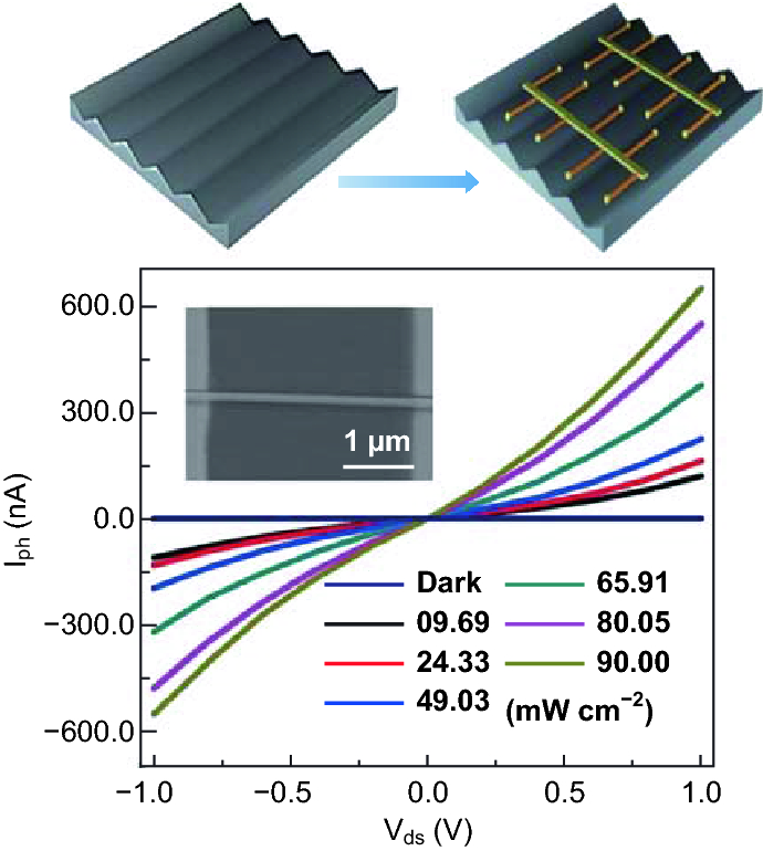
The controllable growth of large area band gap engineered-semiconductor nanowires (NWs) with precise orientation and position is of immense significance in the development of integrated optoelectronic devices. In this study, we have achieved large area in-plane-aligned CdSxSe1−x nanowires via chemical vapor deposition method. The orientation and position of the alloyed CdSxSe1−x NWs could be controlled well by the graphoepitaxial effect and the patterns of Au catalyst. Microstructure characterizations of these as-grown samples reveal that the aligned CdSxSe1−x NWs possess smooth surface and uniform diameter. The aligned CdSxSe1−x NWs have strong photoluminescence and high-quality optical waveguide emission covering almost the entire visible wavelength range. Furthermore, photodetectors were constructed based on individual alloyed CdSxSe1−x NWs. These devices exhibit high performance and fast response speed with photoresponsivity ~ 670 A W−1 and photoresponse time ~ 76 ms. Present work provides a straightforward way to realize in-plane aligned bandgap engineering in semiconductor NWs for the development of large area NW arrays, which exhibit promising applications in future optoelectronic integrated circuits.
Open image in new window
中文翻译:
大面积排列的CdS的可控蒸气生长X硒1−X 用于可见光范围可集成光电探测器的纳米线
摘要
具有精确方向和位置的大面积带隙工程半导体纳米线(NWs)的可控生长在集成光电器件的开发中具有重要意义。在这项研究中,我们已经通过化学气相沉积法获得了大面积的面内排列的CdS x Se 1- x纳米线。合金化的CdS x Se 1- x NWs的取向和位置可以通过石墨外延效应和Au催化剂的图案很好地控制。这些生长样品的微观结构表征表明,对齐的CdS x Se 1- x NWs具有光滑的表面和均匀的直径。对齐的CdS xSe 1- x NW具有强的光致发光和高质量的光波导发射,几乎覆盖了整个可见波长范围。此外,基于单个合金化CdS x Se 1- x NWs构造了光电探测器。这些设备具有高性能和快速响应速度,光响应性约为670 A W -1,光响应时间约为76 ms。当前的工作为在大面积NW阵列的开发中实现半导体NW中的面内对准带隙工程提供了一种直接的方法,该阵列在未来的光电集成电路中显示出有希望的应用。


 京公网安备 11010802027423号