Our official English website, www.x-mol.net, welcomes your
feedback! (Note: you will need to create a separate account there.)
One Second Formation of Large Area Graphene on a Conical Tip Surface via Direct Transformation of Surface Carbide
Small ( IF 13.0 ) Pub Date : 2018-06-25 , DOI: 10.1002/smll.201801288 Yifei Ge 1, 2 , Lele Xu 3 , Xing Lu 3 , Jianxun Xu 2 , Jianbo Liang 1 , Yuliang Zhao 2
Small ( IF 13.0 ) Pub Date : 2018-06-25 , DOI: 10.1002/smll.201801288 Yifei Ge 1, 2 , Lele Xu 3 , Xing Lu 3 , Jianxun Xu 2 , Jianbo Liang 1 , Yuliang Zhao 2
Affiliation
|
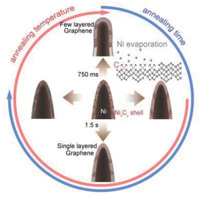
Graphene functionalized nanotips are expected to possess promising potential for various applications based on the outstanding electrical and mechanical properties of graphene. However, current methods, usually requiring a high growth temperature and identical crystal surface to match graphene lattice, are suitable for graphene formation on a flat surface. It remains a big challenge to grow graphene on a nanosized convex surface and fabricate functionalized nanotips with high quality graphene at the apex. In this work, a novel ultrafast annealing method is developed for growing large area graphene on Ni nanotips within 1–2 s. Few layered or multiple layered graphene is presented on the apex or sidewall of the conical tip surface. Direct experimental evidences support that thus‐produced graphene is formed via the direct conversion of nickel carbide at the outer surface under the instantaneous high temperature, which is different from the conventional segregation mechanism. This newly developed ultrafast method provides a new route to produce graphene efficiently and economically, promising for both convex surfaces and flat substrates. Moreover, the graphene functionalized nanotips exhibit a great potential for nanoelectrical measurements and conductive scanning probe microscopy (SPM) applications.
中文翻译:

通过表面碳化物的直接转变在锥形尖端表面上一秒形成大面积石墨烯
基于石墨烯出色的电学和机械性能,石墨烯功能化纳米尖端有望在各种应用中具有广阔的前景。然而,目前的方法通常需要高生长温度和相同的晶体表面来匹配石墨烯晶格,适合在平坦表面上形成石墨烯。在纳米尺寸的凸面上生长石墨烯并制造顶部具有高质量石墨烯的功能化纳米尖端仍然是一个巨大的挑战。在这项工作中,开发了一种新型超快退火方法,可在 1-2 秒内在 Ni 纳米尖端上生长大面积石墨烯。锥形尖端表面的顶点或侧壁上存在少量或多层石墨烯。直接的实验证据表明,由此产生的石墨烯是通过外表面的碳化镍在瞬时高温下直接转化而形成的,这与传统的偏析机制不同。这种新开发的超快方法提供了一种高效、经济地生产石墨烯的新途径,有望用于凸面和平面基材。此外,石墨烯功能化纳米尖端在纳米电测量和导电扫描探针显微镜(SPM)应用中表现出巨大的潜力。
更新日期:2018-06-25
中文翻译:
通过表面碳化物的直接转变在锥形尖端表面上一秒形成大面积石墨烯
基于石墨烯出色的电学和机械性能,石墨烯功能化纳米尖端有望在各种应用中具有广阔的前景。然而,目前的方法通常需要高生长温度和相同的晶体表面来匹配石墨烯晶格,适合在平坦表面上形成石墨烯。在纳米尺寸的凸面上生长石墨烯并制造顶部具有高质量石墨烯的功能化纳米尖端仍然是一个巨大的挑战。在这项工作中,开发了一种新型超快退火方法,可在 1-2 秒内在 Ni 纳米尖端上生长大面积石墨烯。锥形尖端表面的顶点或侧壁上存在少量或多层石墨烯。直接的实验证据表明,由此产生的石墨烯是通过外表面的碳化镍在瞬时高温下直接转化而形成的,这与传统的偏析机制不同。这种新开发的超快方法提供了一种高效、经济地生产石墨烯的新途径,有望用于凸面和平面基材。此外,石墨烯功能化纳米尖端在纳米电测量和导电扫描探针显微镜(SPM)应用中表现出巨大的潜力。


 京公网安备 11010802027423号