当前位置:
X-MOL 学术
›
ACS Photonics
›
论文详情
Our official English website, www.x-mol.net, welcomes your
feedback! (Note: you will need to create a separate account there.)
100 GHz Plasmonic Photodetector
ACS Photonics ( IF 6.5 ) Pub Date : 2018-06-24 00:00:00 , DOI: 10.1021/acsphotonics.8b00525 Yannick Salamin 1 , Ping Ma 1 , Benedikt Baeuerle 1 , Alexandros Emboras 1 , Yuriy Fedoryshyn 1 , Wolfgang Heni 1 , Bojun Cheng 1 , Arne Josten 1 , Juerg Leuthold 1
ACS Photonics ( IF 6.5 ) Pub Date : 2018-06-24 00:00:00 , DOI: 10.1021/acsphotonics.8b00525 Yannick Salamin 1 , Ping Ma 1 , Benedikt Baeuerle 1 , Alexandros Emboras 1 , Yuriy Fedoryshyn 1 , Wolfgang Heni 1 , Bojun Cheng 1 , Arne Josten 1 , Juerg Leuthold 1
Affiliation
|
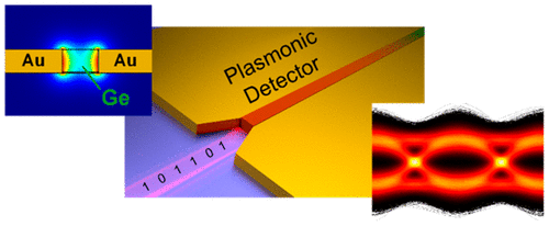
Photodetectors compatible with CMOS technology have shown great potential in implementing active silicon photonics circuits, yet current technologies are facing fundamental bandwidth limitations. Here, we propose and experimentally demonstrate for the first time a plasmonic photodetector achieving simultaneously record-high bandwidth beyond 100 GHz, an internal quantum efficiency of 36% and low footprint. High-speed data reception at 72 Gbit/s is demonstrated. Such superior performance is attributed to the subwavelength confinement of the optical energy in a photoconductive based plasmonic-germanium waveguide detector that enables shortest drift paths for photogenerated carriers and a very small resistance-capacitance product. In addition, the combination of plasmonic structures with absorbing semiconductors enables efficient and highest-speed photodetection. The proposed scheme may pave the way for a cost-efficient CMOS compatible and low temperature fabricated photodetector solution for photodetection beyond 100 Gbit/s, with versatile applications in fields such as communications, microwave photonics, and THz technologies.
中文翻译:

100 GHz等离子光电探测器
与CMOS技术兼容的光电检测器在实现有源硅光子电路方面已显示出巨大的潜力,但当前的技术面临着基本带宽限制。在这里,我们提出并通过实验首次证明了等离激元光电探测器同时实现了超过100 GHz的创纪录高带宽,36%的内部量子效率和低占位面积。演示了72 Gbit / s的高速数据接收。这种优异的性能归因于在基于光电导的等离子体锗波导探测器中光能的亚波长限制,该探测器能够为光生载流子提供最短的漂移路径,并具有非常小的电阻电容乘积。此外,等离子体结构与吸收性半导体的结合可实现高效,最快的光电检测。所提出的方案可以为在100Gbit / s以上的光检测提供具有成本效益的CMOS兼容和低温制造的光检测器解决方案,在通信,微波光子学和THz技术等领域具有广泛的应用。
更新日期:2018-06-24
中文翻译:
100 GHz等离子光电探测器
与CMOS技术兼容的光电检测器在实现有源硅光子电路方面已显示出巨大的潜力,但当前的技术面临着基本带宽限制。在这里,我们提出并通过实验首次证明了等离激元光电探测器同时实现了超过100 GHz的创纪录高带宽,36%的内部量子效率和低占位面积。演示了72 Gbit / s的高速数据接收。这种优异的性能归因于在基于光电导的等离子体锗波导探测器中光能的亚波长限制,该探测器能够为光生载流子提供最短的漂移路径,并具有非常小的电阻电容乘积。此外,等离子体结构与吸收性半导体的结合可实现高效,最快的光电检测。所提出的方案可以为在100Gbit / s以上的光检测提供具有成本效益的CMOS兼容和低温制造的光检测器解决方案,在通信,微波光子学和THz技术等领域具有广泛的应用。


 京公网安备 11010802027423号