Science Bulletin ( IF 18.9 ) Pub Date : 2018-06-15 , DOI: 10.1016/j.scib.2018.06.009 Wenjie Chen 1 , Renrong Liang 1 , Jing Wang 1 , Shuqin Zhang 1 , Jun Xu 1
|
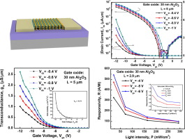
Molybdenum ditelluride (MoTe2) has been demonstrated great potential in electronic and optoelectronic applications. However, the reported effective hole mobility remains far below its theoretical value. Herein, taking advantage of high-κ screening effect, we have fabricated back-gated MoTe2 transistors on an Al2O3 high-κ dielectric and systematically investigated the electronic and optoelectronic properties. A high current on/off ratio exceeding 106 is achieved in the Al2O3-based MoTe2 transistors, and the hole mobility is demonstrated to be 150 cm2 V−1 s−1, compared to 0.2–20 cm2 V−1 s−1 ever obtained from back-gated MoTe2 transistors in the literatures. Moreover, a considerable hole concentration of 1.2 × 1013 cm−2 is attained in our Al2O3-based MoTe2 transistors owing to the strong gate control capability, leading to a high on-state hole current of 6.1 μA μm−1. After optimization, our Al2O3-based MoTe2 phototransistor exhibits outstanding photodetective performance, with a high responsivity of 543 A W−1 and a high photogain of 1,662 at 405 nm light illumination, which are boosted around 419 times compared to the referential SiO2-based control devices. The mechanisms of photoconductivity in the Al2O3-based MoTe2 phototransistors have been analyzed in detail, and the photogating effect is considered to play an important role. This work may provide useful insight to improve carrier mobility in two-dimensional layered semiconductors and open opportunities to facilitate the development of high-performance photodetectors in the future.
中文翻译:
通过使用 Al2O3 高 κ 栅极电介质增强 MoTe2 光电晶体管的光响应性和空穴迁移率
二碲化钼 (MoTe 2 ) 在电子和光电应用中已显示出巨大潜力。然而,报道的有效空穴迁移率仍然远低于其理论值。在此,利用高 κ 屏蔽效应,我们在 Al 2 O 3高 κ 电介质上制备了背栅 MoTe 2晶体管,并系统地研究了其电子和光电特性。在基于 Al 2 O 3的 MoTe 2晶体管中实现了超过 10 6的高电流开/关比,并且证明空穴迁移率为 150 cm 2 V -1 s -1,与文献中从背栅 MoTe 2晶体管获得的0.2–20 cm 2 V −1 s −1相比。此外,由于强大的栅极控制能力,在我们的基于 Al 2 O 3的 MoTe 2晶体管中实现了 1.2 × 10 13 cm -2的相当大的空穴浓度,导致 6.1 μA μm -1的高通态空穴电流. 优化后,我们的基于 Al 2 O 3的 MoTe 2光电晶体管表现出出色的光电探测性能,具有 543 A W −1的高响应度以及在 405 nm 光照下的 1,662 的高光增益,与基于 SiO 2的参考控制设备相比,提升了约 419 倍。详细分析了基于Al 2 O 3的MoTe 2光电晶体管的光电导机制,认为光门效应起着重要作用。这项工作可以为提高二维层状半导体中的载流子迁移率提供有用的见解,并为促进未来高性能光电探测器的发展提供机会。


 京公网安备 11010802027423号