Nano Research ( IF 9.5 ) Pub Date : 2018-06-14 , DOI: 10.1007/s12274-018-2106-9 Ziyao Zhou , Changyong Lan , SenPo Yip , Renjie Wei , Dapan Li , Lei Shu , Johnny C. Ho
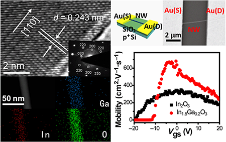
Recently, owing to the excellent electrical and optical properties, n-type In2O3 nanowires (NWs) have attracted tremendous attention for application in memory devices, solar cells, and ultra-violet photodetectors. However, the relatively low electron mobility of In2O3 NWs grown by chemical vapor deposition (CVD) has limited their further utilization. In this study, utilizing in-situ Ga alloying, highly crystalline, uniform, and thin In2xGa2−2xO3 NWs with diameters down to 30 nm were successfully prepared via ambient-pressure CVD. Introducing an optimal amount of Ga (10 at.%) into the In2O3 lattice was found to effectively enhance the crystal quality and reduce the number of oxygen vacancies in the NWs. A further increase in the Ga concentration adversely induced the formation of a resistive β-Ga2O3 phase, thereby deteriorating the electrical properties of the NWs. Importantly, when configured into global back-gated NW field-effect transistors, the optimized In1.8Ga0.2O3 NWs exhibit significantly enhanced electron mobility reaching up to 750 cm2·V–1·s–1 as compared with that of the pure In2O3 NW, which can be attributed to the reduction in the number of oxygen vacancies and ionized impurity scattering centers. Highly ordered NW parallel arrayed devices were also fabricated to demonstrate the versatility and potency of these NWs for next-generation, large-scale, and high-performance nanoelectronics, sensors, etc.
中文翻译:
迈向高机动性
最近,由于出色的电学和光学特性,n型In 2 O 3纳米线(NWs)在存储设备,太阳能电池和紫外线光电探测器中的应用引起了极大的关注。然而,通过化学气相沉积(CVD)生长的In 2 O 3 NW的相对较低的电子迁移率限制了它们的进一步利用。在这项研究中,利用原位Ga合金化,通过环境压力CVD成功地制备了直径低至30 nm的高度结晶,均匀且薄的In 2 x Ga 2−2 x O 3 NW。在In 2中引入最佳量的Ga(10 at。%)发现O 3晶格可有效提高晶体质量并减少NW中的氧空位数量。在Ga浓度的进一步增加的电阻的β-Ga的形成产生不利诱导2 ö 3相,从而降低了纳米线的电性能。重要的是,当配置成全局背栅NW场效应晶体管时,与纯净的In 1.8 Ga 0.2 O 3 NW相比,经过优化的In 1.8 Ga 0.2 O 3 NW表现出显着增强的电子迁移率,达到750 cm 2 ·V –1 ·s –1在2 O 3NW,这可以归因于氧空位和离子化杂质散射中心数量的减少。还制造了高度有序的NW并行阵列器件,以展示这些NW在下一代,大规模和高性能纳米电子器件,传感器等方面的多功能性和效力。


 京公网安备 11010802027423号