Our official English website, www.x-mol.net, welcomes your
feedback! (Note: you will need to create a separate account there.)
Characterization of Single Defects in Ultrascaled MoS2 Field-Effect Transistors
ACS Nano ( IF 15.8 ) Pub Date : 2018-06-07 00:00:00 , DOI: 10.1021/acsnano.8b00268 Bernhard Stampfer 1 , Feng Zhang 2 , Yury Yuryevich Illarionov 1, 3 , Theresia Knobloch 1 , Peng Wu 2 , Michael Waltl 1 , Alexander Grill 1 , Joerg Appenzeller 2 , Tibor Grasser 1
ACS Nano ( IF 15.8 ) Pub Date : 2018-06-07 00:00:00 , DOI: 10.1021/acsnano.8b00268 Bernhard Stampfer 1 , Feng Zhang 2 , Yury Yuryevich Illarionov 1, 3 , Theresia Knobloch 1 , Peng Wu 2 , Michael Waltl 1 , Alexander Grill 1 , Joerg Appenzeller 2 , Tibor Grasser 1
Affiliation
|
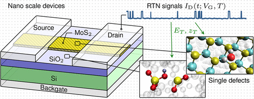
MoS2 has received a lot of attention lately as a semiconducting channel material for electronic devices, in part due to its large band gap as compared to that of other 2D materials. Yet, the performance and reliability of these devices are still severely limited by defects which act as traps for charge carriers, causing severely reduced mobilities, hysteresis, and long-term drift. Despite their importance, these defects are only poorly understood. One fundamental problem in defect characterization is that due to the large defect concentration only the average response to bias changes can be measured. On the basis of such averaged data, a detailed analysis of their properties and identification of particular defect types are difficult. To overcome this limitation, we here characterize single defects on MoS2 devices by performing measurements on ultrascaled transistors (∼65 × 50 nm) which contain only a few defects. These single defects are characterized electrically at varying gate biases and temperatures. The measured currents contain random telegraph noise, which is due to the transfer of charge between the channel of the transistors and individual defects, visible only due to the large impact of a single elementary charge on the local electrostatics in these small devices. Using hidden Markov models for statistical analysis, we extract the charge capture and emission times of a number of defects. By comparing the bias-dependence of the measured capture and emission times to the prediction of theoretical models, we provide simple rules to distinguish oxide traps from adsorbates on these back-gated devices. In addition, we give simple expressions to estimate the vertical and energetic positions of the defects. Using the methods presented in this work, it is possible to locate the sources of performance and reliability limitations in 2D devices and to probe defect distributions in oxide materials with 2D channel materials.
中文翻译:

超大规模MoS 2场效应晶体管中单个缺陷的表征
MoS 2最近作为电子设备的半导体通道材料受到了广泛的关注,部分原因是与其他2D材料相比,MoS 2的带隙大。但是,这些器件的性能和可靠性仍然受到缺陷的严重限制,这些缺陷会充当电荷载流子的陷阱,从而导致迁移率,磁滞和长期漂移严重降低。尽管它们很重要,但对这些缺陷的了解却很少。缺陷表征中的一个基本问题是,由于缺陷浓度较高,因此只能测量对偏差变化的平均响应。基于这样的平均数据,很难对其特性进行详细分析并确定特定的缺陷类型。为了克服这个限制,我们在这里描述MoS上的单个缺陷2个通过对仅包含少量缺陷的超大规模晶体管(〜65×50 nm)进行测量来实现对器件的测量。这些单一缺陷在变化的栅极偏置和温度下具有电气特性。测得的电流包含随机的电报噪声,这是由于晶体管的沟道之间的电荷转移和单个缺陷所致,仅由于单个基本电荷对这些小型设备中的局部静电的巨大影响才可见。使用隐马尔可夫模型进行统计分析,我们提取了许多缺陷的电荷捕获和发射时间。通过将捕获的捕获时间和发射时间与理论模型的预测之间的偏差相关性进行比较,我们提供了简单的规则来区分氧化物陷阱与这些背栅装置上的吸附物。此外,我们给出简单的表达式来估计缺陷的垂直位置和能量位置。使用这项工作中提出的方法,可以在2D器件中定位性能和可靠性限制的来源,并使用2D通道材料探测氧化物材料中的缺陷分布。
更新日期:2018-06-07
中文翻译:
超大规模MoS 2场效应晶体管中单个缺陷的表征
MoS 2最近作为电子设备的半导体通道材料受到了广泛的关注,部分原因是与其他2D材料相比,MoS 2的带隙大。但是,这些器件的性能和可靠性仍然受到缺陷的严重限制,这些缺陷会充当电荷载流子的陷阱,从而导致迁移率,磁滞和长期漂移严重降低。尽管它们很重要,但对这些缺陷的了解却很少。缺陷表征中的一个基本问题是,由于缺陷浓度较高,因此只能测量对偏差变化的平均响应。基于这样的平均数据,很难对其特性进行详细分析并确定特定的缺陷类型。为了克服这个限制,我们在这里描述MoS上的单个缺陷2个通过对仅包含少量缺陷的超大规模晶体管(〜65×50 nm)进行测量来实现对器件的测量。这些单一缺陷在变化的栅极偏置和温度下具有电气特性。测得的电流包含随机的电报噪声,这是由于晶体管的沟道之间的电荷转移和单个缺陷所致,仅由于单个基本电荷对这些小型设备中的局部静电的巨大影响才可见。使用隐马尔可夫模型进行统计分析,我们提取了许多缺陷的电荷捕获和发射时间。通过将捕获的捕获时间和发射时间与理论模型的预测之间的偏差相关性进行比较,我们提供了简单的规则来区分氧化物陷阱与这些背栅装置上的吸附物。此外,我们给出简单的表达式来估计缺陷的垂直位置和能量位置。使用这项工作中提出的方法,可以在2D器件中定位性能和可靠性限制的来源,并使用2D通道材料探测氧化物材料中的缺陷分布。


 京公网安备 11010802027423号