Our official English website, www.x-mol.net, welcomes your
feedback! (Note: you will need to create a separate account there.)
Fermi Level Manipulation through Native Doping in the Topological Insulator Bi2Se3
ACS Nano ( IF 15.8 ) Pub Date : 2018-06-06 00:00:00 , DOI: 10.1021/acsnano.8b03414 Lee A. Walsh 1, 2 , Avery J. Green 3 , Rafik Addou 1 , Westly Nolting 3 , Christopher R. Cormier 1 , Adam T. Barton 1 , Tyler R. Mowll 3 , Ruoyu Yue 1 , Ning Lu 1 , Jiyoung Kim 1 , Moon J. Kim 1 , Vincent P. LaBella 3 , Carl A. Ventrice 3 , Stephen McDonnell 4 , William G. Vandenberghe 1 , Robert M. Wallace 1 , Alain Diebold 3 , Christopher L. Hinkle 1
ACS Nano ( IF 15.8 ) Pub Date : 2018-06-06 00:00:00 , DOI: 10.1021/acsnano.8b03414 Lee A. Walsh 1, 2 , Avery J. Green 3 , Rafik Addou 1 , Westly Nolting 3 , Christopher R. Cormier 1 , Adam T. Barton 1 , Tyler R. Mowll 3 , Ruoyu Yue 1 , Ning Lu 1 , Jiyoung Kim 1 , Moon J. Kim 1 , Vincent P. LaBella 3 , Carl A. Ventrice 3 , Stephen McDonnell 4 , William G. Vandenberghe 1 , Robert M. Wallace 1 , Alain Diebold 3 , Christopher L. Hinkle 1
Affiliation
|
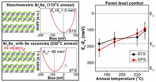
The topologically protected surface states of three-dimensional (3D) topological insulators have the potential to be transformative for high-performance logic and memory devices by exploiting their specific properties such as spin-polarized current transport and defect tolerance due to suppressed backscattering. However, topological insulator based devices have been underwhelming to date primarily due to the presence of parasitic issues. An important example is the challenge of suppressing bulk conduction in Bi2Se3 and achieving Fermi levels (EF) that reside in between the bulk valence and conduction bands so that the topologically protected surface states dominate the transport. The overwhelming majority of the Bi2Se3 studies in the literature report strongly n-type materials with EF in the bulk conduction band due to the presence of a high concentration of selenium vacancies. In contrast, here we report the growth of near-intrinsic Bi2Se3 with a minimal Se vacancy concentration providing a Fermi level near midgap with no extrinsic counter-doping required. We also demonstrate the crucial ability to tuneEF from below midgap into the upper half of the gap near the conduction band edge by controlling the Se vacancy concentration using post-growth anneals. Additionally, we demonstrate the ability to maintain this Fermi level control following the careful, low-temperature removal of a protective Se cap, which allows samples to be transported in air for device fabrication. Thus, we provide detailed guidance for EF control that will finally enable researchers to fabricate high-performance devices that take advantage of transport through the topologically protected surface states of Bi2Se3.
中文翻译:

通过拓扑绝缘体Bi 2 Se 3中的自然掺杂来操纵费米能级。
三维(3D)拓扑绝缘体的受拓扑保护的表面状态具有潜力,可通过利用其特定属性(例如自旋极化电流传输和由于抑制了反向散射的缺陷容忍度)而转变为高性能逻辑和存储设备。但是,迄今为止,基于拓扑绝缘子的设备一直不受欢迎,这主要是由于存在寄生问题。一个重要的例子是挑战,要抑制Bi 2 Se 3中的本体传导并达到存在于本体价态和导带之间的费米能级(E F),以使受拓扑保护的表面态主导传输。绝大多数的Bi 2 Se文献中的3项研究报道,由于存在高浓度的硒空位,在体导带中具有E F的强n型材料。相比之下,这里我们报道了近本征Bi 2 Se 3的生长,其中Se的空位浓度最小,提供了中能隙附近的费米能级,而无需进行外在反掺杂。我们还展示了调节E F的关键能力通过使用生长后退火控制硒的空位浓度,从中间间隙的下方到导带边缘附近间隙的上半部分。此外,我们展示了在小心,低温下移除保护性Se帽之后,能够维持此费米液位控制的能力,该功能使样品能够在空气中运输以进行器件制造。因此,我们为E F控制提供了详细的指导,最终将使研究人员能够制造高性能器件,该器件利用通过Bi 2 Se 3的拓扑受保护的表面态进行传输的优势。
更新日期:2018-06-06
中文翻译:
通过拓扑绝缘体Bi 2 Se 3中的自然掺杂来操纵费米能级。
三维(3D)拓扑绝缘体的受拓扑保护的表面状态具有潜力,可通过利用其特定属性(例如自旋极化电流传输和由于抑制了反向散射的缺陷容忍度)而转变为高性能逻辑和存储设备。但是,迄今为止,基于拓扑绝缘子的设备一直不受欢迎,这主要是由于存在寄生问题。一个重要的例子是挑战,要抑制Bi 2 Se 3中的本体传导并达到存在于本体价态和导带之间的费米能级(E F),以使受拓扑保护的表面态主导传输。绝大多数的Bi 2 Se文献中的3项研究报道,由于存在高浓度的硒空位,在体导带中具有E F的强n型材料。相比之下,这里我们报道了近本征Bi 2 Se 3的生长,其中Se的空位浓度最小,提供了中能隙附近的费米能级,而无需进行外在反掺杂。我们还展示了调节E F的关键能力通过使用生长后退火控制硒的空位浓度,从中间间隙的下方到导带边缘附近间隙的上半部分。此外,我们展示了在小心,低温下移除保护性Se帽之后,能够维持此费米液位控制的能力,该功能使样品能够在空气中运输以进行器件制造。因此,我们为E F控制提供了详细的指导,最终将使研究人员能够制造高性能器件,该器件利用通过Bi 2 Se 3的拓扑受保护的表面态进行传输的优势。


 京公网安备 11010802027423号