Organic Electronics ( IF 2.7 ) Pub Date : 2018-05-22 , DOI: 10.1016/j.orgel.2018.05.032 C. Liewald , S. Strohmair , H. Hecht , E.D. Głowacki , B. Nickel
|
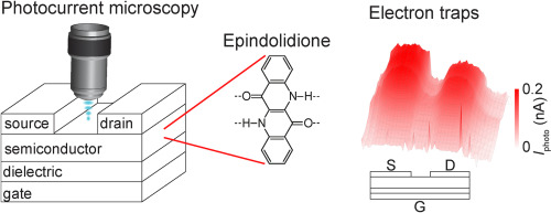
Photocurrent microscopy is used to characterize the kinetics of electrons and holes in organic field-effect transistors (FETs) with the hydrogen-bonded pigment epindolidione as active layer. The method relies on electrons and holes, generated on local illumination, which are provided after exciton splitting, to probe charge trapping. In the dark, hole conduction is observed for negative gate voltage while no electron conduction is observed for positive gate voltage. However, under illumination, a fast displacement current with 60 μs onset time and 1 ms exponential decay occurs for positive gate voltage, which can be explained by exciton splitting underneath the semitransparent top contact followed by subsequent electron trapping and hole extraction. Afterward, trapped electrons hop via further trap states within the film to the insulator into interface traps (13 ms exponential decay) which induce a positive threshold voltage shift in the FET transfer curves for hole transport. Photocurrent microscopy confirms that the displacement current occurs only for illumination under and near the semitransparent source/drain contacts, which act here as metal-insulator-semiconductor (MIS) diodes. For negative gate voltage instead, the photocurrent comprises an enhanced hole current in the FET channel between the contacts. In the channel region, the detrapping of holes at the interface with the insulator (3 ms time constant) enhances the transistor current at low frequencies <1 kHz, whereas the displacement current between the contacts and the gate is observed only at frequencies >10 kHz. Thus, we show here that photocurrent microscopy allows to identify the kinetics of electrons and holes in traps close to the contacts and in the FET channel of pigment transistors.
中文翻译:
颜料半导体表聚二酮中电子和空穴的扫描光电流显微镜检查
光电流显微镜用于表征有机和场效应晶体管(FET)中电子和空穴的动力学,其中氢键合色素表皮二酮为活性层。该方法依靠在激子分裂后提供的局部照明下产生的电子和空穴来探测电荷陷阱。在黑暗中,对于负栅极电压观察到空穴传导,而对于正栅极电压观察不到电子传导。但是,在照明下,对于正的栅极电压,会发生具有60μs的启动时间和1 ms的指数衰减的快速位移电流,这可以通过半透明顶部触点下方的激子分裂,随后的电子俘获和空穴提取来解释。之后,被捕获的电子通过薄膜中的其他陷阱状态跃迁到绝缘体,进入界面陷阱(13 ms指数衰减),从而在FET传输曲线中产生正阈值电压偏移,以进行空穴传输。光电流显微镜证实,位移电流仅发生在半透明源极/漏极触点下方和附近的照明中,在此情况下,其充当金属-绝缘体-半导体(MIS)二极管。相反,对于负栅极电压,光电流在触点之间的FET通道中包含增强的空穴电流。在沟道区,与绝缘体的界面处的空穴释放(3 ms时间常数)在<1 kHz的低频下增强了晶体管电流,而仅在> 10 kHz的频率下才观察到触点和栅极之间的位移电流。 。因此,


 京公网安备 11010802027423号