当前位置:
X-MOL 学术
›
Adv. Funct. Mater.
›
论文详情
Our official English website, www.x-mol.net, welcomes your
feedback! (Note: you will need to create a separate account there.)
High Mobility Anisotropic Black Phosphorus Nanoribbon Field‐Effect Transistor
Advanced Functional Materials ( IF 18.5 ) Pub Date : 2018-05-21 , DOI: 10.1002/adfm.201801524 Xuewei Feng 1, 2 , Xin Huang 1, 2 , Li Chen 1, 2 , Wee Chong Tan 1, 2 , Lin Wang 1, 2 , Kah-Wee Ang 1, 2
Advanced Functional Materials ( IF 18.5 ) Pub Date : 2018-05-21 , DOI: 10.1002/adfm.201801524 Xuewei Feng 1, 2 , Xin Huang 1, 2 , Li Chen 1, 2 , Wee Chong Tan 1, 2 , Lin Wang 1, 2 , Kah-Wee Ang 1, 2
Affiliation
|
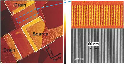
Achieving excellent electrostatic control and immunity to short channel effects are the formidable challenges in ultrascaled devices. 3D device architectures, such as nanoribbon, have successfully mitigated these problems by achieving uniform top‐ and side‐wall control of the channel. Here, by leveraging on the merits of 3D structure, high‐mobility black phosphorus nanoribbon field‐effect transistors (BPNR‐FET) are demonstrated and the anisotropic transport properties are systematically investigated. A simple top‐down reactive ion etching method is used to realize both armchair‐ and zigzag‐oriented nanoribbons with various widths down to 60 nm. The mobility of BPNR‐FET is found to be width‐ and thickness‐dependent, with the highest hole mobility of ≈862 cm2 V−1 s−1 demonstrated in armchair‐oriented device at room temperature by combining high‐κ gate dielectric and hydrogen treatment to reduce sidewall scattering. Furthermore, hydrogenation effectively passivates the nanoribbon dangling bonds, leading to hysteresis and contact resistance improvement. This work unravels the superior electrical performance underscore a conceptually new device based on BP nanoribbons, paving the way toward the development of nonplanar devices on 2D materials platform.
中文翻译:

高迁移率各向异性黑色磷纳米带场效应晶体管
实现出色的静电控制和对短通道效应的抵抗力是超大规模设备面临的巨大挑战。3D设备架构(例如纳米带)已经通过实现通道的顶部和侧壁统一控制而成功缓解了这些问题。在这里,利用3D结构的优点,展示了高迁移率的黑磷纳米带场效应晶体管(BPNR-FET),并系统地研究了各向异性传输特性。一种简单的自上而下的反应性离子蚀刻方法可用于实现宽度小于60 nm的扶手椅状和之字形的纳米带。发现BPNR-FET的迁移率取决于宽度和厚度,最大空穴迁移率约为862 cm 2 V -1 s -1通过结合高κ栅极电介质和氢处理以减少侧壁散射,在室温的扶手椅式设备中得到了证明。此外,氢化有效地钝化了纳米带的悬空键,从而导致磁滞和接触电阻的提高。这项工作揭示了卓越的电气性能,这突显了基于BP纳米带的概念上新颖的设备,为在2D材料平台上开发非平面设备铺平了道路。
更新日期:2018-05-21
中文翻译:
高迁移率各向异性黑色磷纳米带场效应晶体管
实现出色的静电控制和对短通道效应的抵抗力是超大规模设备面临的巨大挑战。3D设备架构(例如纳米带)已经通过实现通道的顶部和侧壁统一控制而成功缓解了这些问题。在这里,利用3D结构的优点,展示了高迁移率的黑磷纳米带场效应晶体管(BPNR-FET),并系统地研究了各向异性传输特性。一种简单的自上而下的反应性离子蚀刻方法可用于实现宽度小于60 nm的扶手椅状和之字形的纳米带。发现BPNR-FET的迁移率取决于宽度和厚度,最大空穴迁移率约为862 cm 2 V -1 s -1通过结合高κ栅极电介质和氢处理以减少侧壁散射,在室温的扶手椅式设备中得到了证明。此外,氢化有效地钝化了纳米带的悬空键,从而导致磁滞和接触电阻的提高。这项工作揭示了卓越的电气性能,这突显了基于BP纳米带的概念上新颖的设备,为在2D材料平台上开发非平面设备铺平了道路。


 京公网安备 11010802027423号