当前位置:
X-MOL 学术
›
Inorg. Chem. Front.
›
论文详情
Our official English website, www.x-mol.net, welcomes your
feedback! (Note: you will need to create a separate account there.)
One-step CVD fabrication and optoelectronic properties of SnS2/SnS vertical heterostructures†
Inorganic Chemistry Frontiers ( IF 6.1 ) Pub Date : 2018-05-21 00:00:00 , DOI: 10.1039/c8qi00251g Mingling Li 1, 2, 3, 4 , Yunsong Zhu 1, 2, 3, 4 , Taishen Li 1, 2, 3, 4 , Yue Lin 1, 2, 3, 4 , Hongbing Cai 1, 2, 3, 4 , Sijia Li 1, 2, 3, 4 , Huaiyi Ding 1, 2, 3, 4 , Nan Pan 1, 2, 3, 4, 5 , Xiaoping Wang 1, 2, 3, 4, 5
Inorganic Chemistry Frontiers ( IF 6.1 ) Pub Date : 2018-05-21 00:00:00 , DOI: 10.1039/c8qi00251g Mingling Li 1, 2, 3, 4 , Yunsong Zhu 1, 2, 3, 4 , Taishen Li 1, 2, 3, 4 , Yue Lin 1, 2, 3, 4 , Hongbing Cai 1, 2, 3, 4 , Sijia Li 1, 2, 3, 4 , Huaiyi Ding 1, 2, 3, 4 , Nan Pan 1, 2, 3, 4, 5 , Xiaoping Wang 1, 2, 3, 4, 5
Affiliation
|
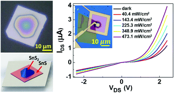
Heterostructures constructed by two-dimensional (2D) material layers, which are usually prepared via a transfer/stacking method or van der Waals epitaxy, have achieved significant success in various optoelectronic devices including solar cells, light-emitting diodes and photodetectors. However, to date, most of these heterostructures comprise 2D materials with a similar crystal structure. Thus, preparation of heterostructures with different crystal structures is desirable but still a great challenge. Herein, we report a one-step CVD strategy to successfully grow SnS2/SnS vertical heterostructures on a mica substrate. Raman spectroscopy, atomic force microscopy (AFM) and transmission electron microscopy (TEM) characterizations reveal that the heterostructure is formed by stacking of pyramid-shaped SnS2 of the hexagonal structure onto the rhombus SnS flake of the orthorhombic structure. The photodetector based on the SnS2/SnS heterostructure demonstrates high optoelectronic performance: a 27.7 A W−1 photoresponsivity, 2.2 × 10³ on/off ratio, less than 10 ms response time and 2.1 × 10¹⁰ jones specific detectivity. The superior performance originates from the high crystal quality of the as-grown heterostructure and its vertical device architecture. This study can expand our capability to fabricate a variety of two-dimensional heterostructures and make these heterostructures highly desirable as novel building blocks for potential applications in electronic and optoelectronic devices.
中文翻译:

SnS 2 / SnS垂直异质结构的一步式CVD制备和光电性能†
通常通过转移/堆叠方法或范德华外延法制备的由二维(2D)材料层构成的异质结构已在包括太阳能电池,发光二极管和光电探测器在内的各种光电设备中取得了巨大的成功。然而,迄今为止,这些异质结构中的大多数都包含具有相似晶体结构的2D材料。因此,期望制备具有不同晶体结构的异质结构,但是仍然是巨大的挑战。在此,我们报告了一步法CVD策略以成功生长SnS 2云母基底上的/ SnS垂直异质结构。拉曼光谱,原子力显微镜(AFM)和透射电子显微镜(TEM)表征表明,异质结构是通过将六边形结构的金字塔形状的SnS 2堆叠到正交结构的菱形SnS薄片上而形成的。基于SnS 2 / SnS异质结构的光电检测器显示出高光电性能:27.7 AW -1光响应度,2.2×10 3开/关比,不到10 ms的响应时间和2.1×10 10琼斯特有的侦探性。优异的性能源于所生长异质结构的高晶体质量及其垂直器件架构。这项研究可以扩展我们制造各种二维异质结构的能力,并使这些异质结构成为电子和光电子设备中潜在应用的新型构建基块非常理想。
更新日期:2018-05-21
中文翻译:
SnS 2 / SnS垂直异质结构的一步式CVD制备和光电性能†
通常通过转移/堆叠方法或范德华外延法制备的由二维(2D)材料层构成的异质结构已在包括太阳能电池,发光二极管和光电探测器在内的各种光电设备中取得了巨大的成功。然而,迄今为止,这些异质结构中的大多数都包含具有相似晶体结构的2D材料。因此,期望制备具有不同晶体结构的异质结构,但是仍然是巨大的挑战。在此,我们报告了一步法CVD策略以成功生长SnS 2云母基底上的/ SnS垂直异质结构。拉曼光谱,原子力显微镜(AFM)和透射电子显微镜(TEM)表征表明,异质结构是通过将六边形结构的金字塔形状的SnS 2堆叠到正交结构的菱形SnS薄片上而形成的。基于SnS 2 / SnS异质结构的光电检测器显示出高光电性能:27.7 AW -1光响应度,2.2×10 3开/关比,不到10 ms的响应时间和2.1×10 10琼斯特有的侦探性。优异的性能源于所生长异质结构的高晶体质量及其垂直器件架构。这项研究可以扩展我们制造各种二维异质结构的能力,并使这些异质结构成为电子和光电子设备中潜在应用的新型构建基块非常理想。


 京公网安备 11010802027423号