当前位置:
X-MOL 学术
›
Adv. Funct. Mater.
›
论文详情
Our official English website, www.x-mol.net, welcomes your
feedback! (Note: you will need to create a separate account there.)
Evidence for Chemicals Intermingling at Silicon/Titanium Oxide (TiOx) Interface and Existence of Multiple Bonding States in Monolithic TiOx
Advanced Functional Materials ( IF 18.5 ) Pub Date : 2018-05-18 , DOI: 10.1002/adfm.201707018 Neeraj Dwivedi 1 , Reuben J. Yeo 2 , Hui R. Tan 3 , Rolf Stangl 4 , Armin G. Aberle 4 , Charanjit S. Bhatia 1 , Aaron Danner 1 , Baochen Liao 4
Advanced Functional Materials ( IF 18.5 ) Pub Date : 2018-05-18 , DOI: 10.1002/adfm.201707018 Neeraj Dwivedi 1 , Reuben J. Yeo 2 , Hui R. Tan 3 , Rolf Stangl 4 , Armin G. Aberle 4 , Charanjit S. Bhatia 1 , Aaron Danner 1 , Baochen Liao 4
Affiliation
|
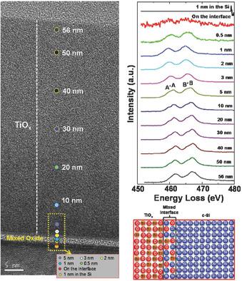
Metal oxides (MOs) are used in photovoltaics and microelectronics as surface passivating layers and gate dielectrics, respectively. The effectiveness of MOs predominantly depends on their structure and the nature of the semiconductor/MO (S/MO) interface. While some efforts are made to analyze interface behavior of a few MOs, greater fundamental understanding on the interface and structural behaviors of emerging MOs is yet to be established for enhanced scientific and technological developments. Here, the structure of atomic layer deposited titanium oxide (TiOx) and the nature of the c‐Si/TiOx interface on the atomic‐ to nanoscale are probed. A new breed of mixed oxide (SiOx+TiOx) interfacial layer with a thickness of ≈1.3 nm at the c‐Si/TiOx interface is discovered, and its thickness further increases to ≈1.5 nm after postdeposition annealing. It is observed that both as‐deposited and annealed monolithic TiOx films comprise multiple bonding states at varying film thickness, with an oxygen‐deficient TiOx layer located close to the mixed oxide/TiOx interface. The stoichiometry of this layer improves when reaching the middle and near surface regions of the TiOx layer, respectively. This work uncovers several critical structural and interface aspects of TiOx, and thus creates opportunities to control and design improved photovoltaic and electronic devices for future development.
中文翻译:

化学品混入硅/钛氧化物(TiOx)界面的证据以及整体TiOx中多个键合状态的存在
金属氧化物(MO)分别用于光伏和微电子领域,作为表面钝化层和栅极电介质。MO的有效性主要取决于它们的结构和半导体/ MO(S / MO)接口的性质。尽管已经做出了一些努力来分析几个MO的界面行为,但是对于新兴的MO的界面和结构行为,人们还需要建立更多的基础知识,以促进科学技术的发展。在此,探讨了原子层沉积的二氧化钛(TiO x)的结构以及原子级至纳米级的c-Si / TiO x界面的性质。新型混合氧化物(SiO x + TiO x)发现在c-Si / TiO x界面处的界面层厚度约为1.3 nm,沉积后退火后其厚度进一步增加至≈1.5 nm。可以观察到,沉积和退火的整体式TiO x膜在不同的膜厚度下均具有多种键合状态,缺氧的TiO x层位于混合氧化物/ TiO x混合界面附近。当分别到达TiO x层的中和近表面区域时,该层的化学计量提高。这项工作揭示了TiO x的几个关键的结构和界面方面,从而为控制和设计经过改进的光伏和电子设备,为将来的发展创造了机会。
更新日期:2018-05-18
中文翻译:
化学品混入硅/钛氧化物(TiOx)界面的证据以及整体TiOx中多个键合状态的存在
金属氧化物(MO)分别用于光伏和微电子领域,作为表面钝化层和栅极电介质。MO的有效性主要取决于它们的结构和半导体/ MO(S / MO)接口的性质。尽管已经做出了一些努力来分析几个MO的界面行为,但是对于新兴的MO的界面和结构行为,人们还需要建立更多的基础知识,以促进科学技术的发展。在此,探讨了原子层沉积的二氧化钛(TiO x)的结构以及原子级至纳米级的c-Si / TiO x界面的性质。新型混合氧化物(SiO x + TiO x)发现在c-Si / TiO x界面处的界面层厚度约为1.3 nm,沉积后退火后其厚度进一步增加至≈1.5 nm。可以观察到,沉积和退火的整体式TiO x膜在不同的膜厚度下均具有多种键合状态,缺氧的TiO x层位于混合氧化物/ TiO x混合界面附近。当分别到达TiO x层的中和近表面区域时,该层的化学计量提高。这项工作揭示了TiO x的几个关键的结构和界面方面,从而为控制和设计经过改进的光伏和电子设备,为将来的发展创造了机会。


 京公网安备 11010802027423号