当前位置:
X-MOL 学术
›
Mater. Horiz.
›
论文详情
Our official English website, www.x-mol.net, welcomes your
feedback! (Note: you will need to create a separate account there.)
Electron tunneling through grain boundaries in transparent conductive oxides and implications for electrical conductivity: the case of ZnO:Al thin films†
Materials Horizons ( IF 12.2 ) Pub Date : 2018-05-17 00:00:00 , DOI: 10.1039/c8mh00402a Viet Huong Nguyen 1, 2, 3, 4, 5 , Ulrich Gottlieb 1, 2, 3, 4, 5 , Anthony Valla 1, 6, 7, 8, 9 , Delfina Muñoz 1, 6, 7, 8, 9 , Daniel Bellet 1, 2, 3, 4, 5 , David Muñoz-Rojas 1, 2, 3, 4, 5
Materials Horizons ( IF 12.2 ) Pub Date : 2018-05-17 00:00:00 , DOI: 10.1039/c8mh00402a Viet Huong Nguyen 1, 2, 3, 4, 5 , Ulrich Gottlieb 1, 2, 3, 4, 5 , Anthony Valla 1, 6, 7, 8, 9 , Delfina Muñoz 1, 6, 7, 8, 9 , Daniel Bellet 1, 2, 3, 4, 5 , David Muñoz-Rojas 1, 2, 3, 4, 5
Affiliation
|
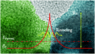
In this work, we have applied the Airy Function Transfer-Matrix Method to provide a numerical description of the charge scattering mechanisms taking place at the grain boundaries in polycrystalline, degenerately Al-doped ZnO (ZnO:Al) films, one of the most studied Transparent Conductive Oxides (TCOs). By discretizing the potential barrier at the grain boundary into linear segments, an accurate calculation of the electron tunneling probability through the grain boundaries has been obtained. Conversely to analytical models based on the Wentzel–Kramers–Brillouin (WKB) approximation, our new approach is valid for any doping level. We thus provide a complete model that allows a comprehensive explanation of carrier transport in highly doped semiconductors, for which charge tunneling across grain boundaries cannot be neglected. We have tested our model with ZnO:Al thin films prepared by different physical and chemical deposition techniques, namely, sputtering, atomic layer deposition and atmospheric pressure spatial atomic layer deposition. A linear relationship between the trap density at the grain boundaries and carrier density has been extracted by fitting our model to Hall mobility data for the different samples. Our results provide guidance on how to adapt the deposition conditions to obtain high-quality materials, with an optimum ratio between optical and electrical properties as required for specific applications.
中文翻译:

电子在透明导电氧化物中穿过晶界的隧穿及其对电导率的影响:ZnO:Al薄膜的情况†
在这项工作中,我们应用了艾里函数传递矩阵方法,对在多晶,简并掺铝的ZnO(ZnO:Al)薄膜中晶界处发生的电荷散射机理进行了数值描述,这是研究最多的薄膜之一透明导电氧化物(TCO)。通过将晶界处的势垒离散化成线性段,已经获得了通过晶界的电子隧穿概率的精确计算。与基于Wentzel-Kramers-Brillouin(WKB)近似的分析模型相反,我们的新方法适用于任何掺杂水平。因此,我们提供了一个完整的模型,可以对高掺杂半导体中的载流子传输进行全面的解释,因为对于载流子,不能忽略跨晶界的电荷隧穿。我们已经用通过不同物理和化学沉积技术(即溅射,原子层沉积和大气压空间原子层沉积)制备的ZnO:Al薄膜测试了我们的模型。通过将我们的模型拟合为不同样品的霍尔迁移率数据,可以提取出晶界处陷阱能级与载流子密度之间的线性关系。我们的结果为如何适应沉积条件以获得高质量的材料提供了指导,并根据特定应用的要求在光学和电学性质之间实现了最佳比例。通过将我们的模型拟合为不同样品的霍尔迁移率数据,可以提取出晶界处陷阱能级与载流子密度之间的线性关系。我们的结果为如何适应沉积条件以获得高质量的材料提供了指导,并根据特定应用的需要在光学和电学性质之间实现了最佳比例。通过将我们的模型拟合为不同样品的霍尔迁移率数据,可以提取出晶界处陷阱能级与载流子密度之间的线性关系。我们的结果为如何适应沉积条件以获得高质量的材料提供了指导,并根据特定应用的需要在光学和电学性质之间实现了最佳比例。
更新日期:2018-05-17
中文翻译:
电子在透明导电氧化物中穿过晶界的隧穿及其对电导率的影响:ZnO:Al薄膜的情况†
在这项工作中,我们应用了艾里函数传递矩阵方法,对在多晶,简并掺铝的ZnO(ZnO:Al)薄膜中晶界处发生的电荷散射机理进行了数值描述,这是研究最多的薄膜之一透明导电氧化物(TCO)。通过将晶界处的势垒离散化成线性段,已经获得了通过晶界的电子隧穿概率的精确计算。与基于Wentzel-Kramers-Brillouin(WKB)近似的分析模型相反,我们的新方法适用于任何掺杂水平。因此,我们提供了一个完整的模型,可以对高掺杂半导体中的载流子传输进行全面的解释,因为对于载流子,不能忽略跨晶界的电荷隧穿。我们已经用通过不同物理和化学沉积技术(即溅射,原子层沉积和大气压空间原子层沉积)制备的ZnO:Al薄膜测试了我们的模型。通过将我们的模型拟合为不同样品的霍尔迁移率数据,可以提取出晶界处陷阱能级与载流子密度之间的线性关系。我们的结果为如何适应沉积条件以获得高质量的材料提供了指导,并根据特定应用的要求在光学和电学性质之间实现了最佳比例。通过将我们的模型拟合为不同样品的霍尔迁移率数据,可以提取出晶界处陷阱能级与载流子密度之间的线性关系。我们的结果为如何适应沉积条件以获得高质量的材料提供了指导,并根据特定应用的需要在光学和电学性质之间实现了最佳比例。通过将我们的模型拟合为不同样品的霍尔迁移率数据,可以提取出晶界处陷阱能级与载流子密度之间的线性关系。我们的结果为如何适应沉积条件以获得高质量的材料提供了指导,并根据特定应用的需要在光学和电学性质之间实现了最佳比例。


 京公网安备 11010802027423号