当前位置:
X-MOL 学术
›
J. Phys. Chem. C
›
论文详情
Our official English website, www.x-mol.net, welcomes your
feedback! (Note: you will need to create a separate account there.)
Synthesis and Material Properties of Bi2Se3 Nanostructures Deposited by SILAR
The Journal of Physical Chemistry C ( IF 3.3 ) Pub Date : 2018-05-10 00:00:00 , DOI: 10.1021/acs.jpcc.8b01692 Rasin Ahmed 1 , Yin Xu 1 , Maria Gabriela Sales 1 , Qiyuan Lin 1 , Stephen McDonnell 1 , Giovanni Zangari 1
The Journal of Physical Chemistry C ( IF 3.3 ) Pub Date : 2018-05-10 00:00:00 , DOI: 10.1021/acs.jpcc.8b01692 Rasin Ahmed 1 , Yin Xu 1 , Maria Gabriela Sales 1 , Qiyuan Lin 1 , Stephen McDonnell 1 , Giovanni Zangari 1
Affiliation
|
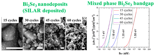
Bi2Se3 was synthesized by a room-temperature deposition technique and successive ionic layer adsorption and reaction (SILAR) method with the aim to understand the formation, crystallinity, optical properties, and energy band structure of this material. The Bi2Se3 morphology was found to change from nanoparticles to that of a nanocluster network by increasing the SILAR deposition cycles. The crystalline structure of as-prepared Bi2Se3 determined from the grazing-incidence X-ray diffraction (GI-XRD) pattern was found to have a mixed of metastable orthorhombic and rhombohedral phases which was further confirmed from our analysis of the Raman spectra. The optical bandgap of Bi2Se3 varied from 1.58 to 1.05 eV for 15–90 cycles of deposition, in contrast to the semimetallic 0.3 eV bandgap exhibited by the pure rhombohedral phase. A schematic band diagram of Bi2Se3 prepared by 45 SILAR cycles was constructed for the mixed-phase Bi2Se3. The flat-band potential was determined to be at 0.46 V vs. RHE from Mott–Schottky analysis. Low-temperature annealing at 100 °C for 1 h resulted in the improvement of the rhombohedral phase fraction which was confirmed from analysis of GI-XRD pattern and pronounced E2g and A21g bulk vibrational modes in the Raman spectrum. The absorption cutoff after annealing was found to be red-shifted combined with a sub-bandgap absorption above 0.78 eV. The post-annealing results indicated the onset of an early stage transition from semiconductor to semi-metallic properties for Bi2Se3.
中文翻译:

SILAR沉积的Bi 2 Se 3纳米结构的合成与材料性能
Bi 2 Se 3是通过室温沉积技术和连续的离子层吸附和反应(SILAR)方法合成的,目的是了解这种材料的形成,结晶度,光学性质和能带结构。发现Bi 2 Se 3的形态通过增加SILAR沉积周期而从纳米粒子变为纳米簇网络。发现由掠入射X射线衍射(GI-XRD)模式确定的制备的Bi 2 Se 3的晶体结构具有亚稳态的正交晶相和菱面体相的混合物,这从我们对拉曼光谱的分析中得到了进一步证实。Bi的光学带隙2 Se 3在15-90个沉积循环中的变化范围为1.58至1.05 eV,这与纯菱形面相表现出的半金属0.3 eV带隙相反。对于混合相Bi 2 Se 3,通过45个SILAR循环制备了Bi 2 Se 3的示意性能带图。根据Mott–Schottky分析,相对于RHE,平带电势确定为0.46V。通过GI-XRD图谱分析以及明显的E 2 g和A 2 1g在100°C的低温退火1 h导致菱面体相分数的改善。拉曼光谱中的体振动模式。发现退火后的吸收截止值发生了红移,同时亚带隙吸收超过0.78 eV。退火后的结果表明Bi 2 Se 3从半导体性质向半金属性质的早期转变的开始。
更新日期:2018-05-10
中文翻译:
SILAR沉积的Bi 2 Se 3纳米结构的合成与材料性能
Bi 2 Se 3是通过室温沉积技术和连续的离子层吸附和反应(SILAR)方法合成的,目的是了解这种材料的形成,结晶度,光学性质和能带结构。发现Bi 2 Se 3的形态通过增加SILAR沉积周期而从纳米粒子变为纳米簇网络。发现由掠入射X射线衍射(GI-XRD)模式确定的制备的Bi 2 Se 3的晶体结构具有亚稳态的正交晶相和菱面体相的混合物,这从我们对拉曼光谱的分析中得到了进一步证实。Bi的光学带隙2 Se 3在15-90个沉积循环中的变化范围为1.58至1.05 eV,这与纯菱形面相表现出的半金属0.3 eV带隙相反。对于混合相Bi 2 Se 3,通过45个SILAR循环制备了Bi 2 Se 3的示意性能带图。根据Mott–Schottky分析,相对于RHE,平带电势确定为0.46V。通过GI-XRD图谱分析以及明显的E 2 g和A 2 1g在100°C的低温退火1 h导致菱面体相分数的改善。拉曼光谱中的体振动模式。发现退火后的吸收截止值发生了红移,同时亚带隙吸收超过0.78 eV。退火后的结果表明Bi 2 Se 3从半导体性质向半金属性质的早期转变的开始。


 京公网安备 11010802027423号