当前位置:
X-MOL 学术
›
Small Methods
›
论文详情
Our official English website, www.x-mol.net, welcomes your
feedback! (Note: you will need to create a separate account there.)
Light Sources and Photodetectors Enabled by 2D Semiconductors
Small Methods ( IF 10.7 ) Pub Date : 2018-05-02 , DOI: 10.1002/smtd.201800019 Jingzhi Shang 1, 2 , Chunxiao Cong 3 , Lishu Wu 2 , Wei Huang 1, 4 , Ting Yu 2
Small Methods ( IF 10.7 ) Pub Date : 2018-05-02 , DOI: 10.1002/smtd.201800019 Jingzhi Shang 1, 2 , Chunxiao Cong 3 , Lishu Wu 2 , Wei Huang 1, 4 , Ting Yu 2
Affiliation
|
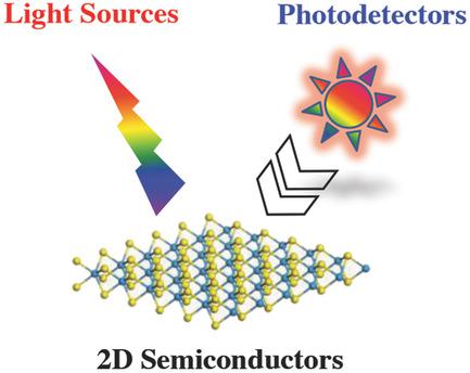
The emerging 2D semiconductors have aroused increasing attention due to their fascinating fundamental properties and application prospects. Technical investigation of 2D semiconductor–based electronics and optoelectronics is paving the way to realizing practical applications, which opens up new opportunities to reshape the current semiconductor industry. Particularly, 2D semiconductor–based optoelectronics can be extensively utilized in the promising semiconductor and information industries, such as solid‐state lighting, on‐chip optical interconnects, quantum computing, and communication. Here, the research progress regarding the fabrication and characterization of rapidly growing light‐emitting devices and photodetectors enabled by 2D semiconductors is reviewed. According to different emission mechanisms, 2D semiconductor–activated light sources are classified into four types: excitonic light‐emitting diodes (LEDs), quantum LEDs, valley LEDs, and lasers. Moreover, photodetecting devices based on atomically thin MoS2, other 2D semiconductors, and van der Waals heterostructures are discussed, where diverse device structures, performance parameters, and working principles are compared. Furthermore, the remaining challenges in the realization of practical devices with desirable features are outlined and new research opportunities for 2D semiconductor optoelectronics are proposed.
中文翻译:

二维半导体实现的光源和光电检测器
新兴的2D半导体由于其引人入胜的基本性能和应用前景而引起了越来越多的关注。对基于2D半导体的电子和光电技术的技术研究为实现实际应用铺平了道路,这为重塑当前的半导体行业提供了新的机会。特别是,基于2D半导体的光电技术可广泛应用于有前途的半导体和信息产业,例如固态照明,片上光学互连,量子计算和通信。在此,对有关由2D半导体实现的快速增长的发光器件和光电检测器的制造和表征的研究进展进行了综述。根据不同的排放机制,二维半导体激活光源分为四种类型:激子发光二极管(LED),量子LED,谷底LED和激光器。此外,基于原子稀薄的MoS的光电检测设备参考图2,讨论了其他2D半导体和范德华异质结构,比较了各种器件结构,性能参数和工作原理。此外,概述了在实现具有期望特征的实际装置中的剩余挑战,并提出了用于二维半导体光电子学的新研究机会。
更新日期:2018-05-02
中文翻译:
二维半导体实现的光源和光电检测器
新兴的2D半导体由于其引人入胜的基本性能和应用前景而引起了越来越多的关注。对基于2D半导体的电子和光电技术的技术研究为实现实际应用铺平了道路,这为重塑当前的半导体行业提供了新的机会。特别是,基于2D半导体的光电技术可广泛应用于有前途的半导体和信息产业,例如固态照明,片上光学互连,量子计算和通信。在此,对有关由2D半导体实现的快速增长的发光器件和光电检测器的制造和表征的研究进展进行了综述。根据不同的排放机制,二维半导体激活光源分为四种类型:激子发光二极管(LED),量子LED,谷底LED和激光器。此外,基于原子稀薄的MoS的光电检测设备参考图2,讨论了其他2D半导体和范德华异质结构,比较了各种器件结构,性能参数和工作原理。此外,概述了在实现具有期望特征的实际装置中的剩余挑战,并提出了用于二维半导体光电子学的新研究机会。


 京公网安备 11010802027423号