当前位置:
X-MOL 学术
›
Small Methods
›
论文详情
Our official English website, www.x-mol.net, welcomes your
feedback! (Note: you will need to create a separate account there.)
Interfacial Engineering for Fabricating High‐Performance Field‐Effect Transistors Based on 2D Materials
Small Methods ( IF 10.7 ) Pub Date : 2018-04-30 , DOI: 10.1002/smtd.201700384 Feng Gao 1, 2 , Huihui Yang 1, 2 , PingAn Hu 1, 2
Small Methods ( IF 10.7 ) Pub Date : 2018-04-30 , DOI: 10.1002/smtd.201700384 Feng Gao 1, 2 , Huihui Yang 1, 2 , PingAn Hu 1, 2
Affiliation
|
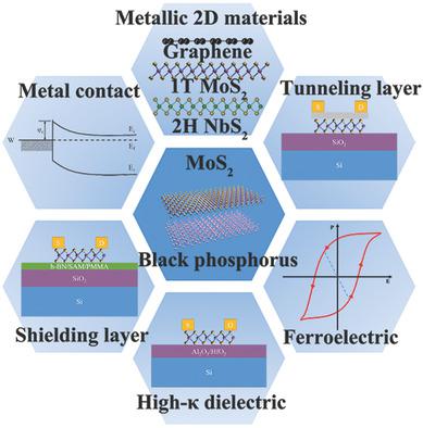
Traditional scaled complementary metal–oxide–semiconductor field‐effects transistors (FETs) are currently approaching physical limitations and are confronted with bottlenecks in their development. The increasing demands of FETs with high electronic performance and integration density have strongly motivated the exploration of novel channel materials, among which 2D materials are emerging as ideal candidates. In particular, 2D materials possess unique immunity to the short channel effects and also facilitate the realization of flexible microelectronic devices. Interface engineering is pivotal for optimizing the performance of traditional electronics, as well as 2D layered semiconductor electronics. So far, enormous efforts have been made to develop high‐performance FETs based on 2D materials. Here, a summary of the recent progress in 2D FET devices is presented, with a focus on the technologies and methodologies of interface engineering in 2D semiconductor FETs. Corresponding strategies are presented, including tuning the Schottky barrier height, optimizing the interface morphology, and so on. In the last part, the possible developing trends for 2D FET devices in the future are discussed.
中文翻译:

基于二维材料的高性能场效应晶体管的界面工程
传统规模化的互补金属氧化物半导体场效应晶体管(FET)目前正接近物理极限,并且在发展过程中面临瓶颈。对具有高电子性能和集成密度的FET的不断增长的需求,极大地推动了对新型沟道材料的探索,其中2D材料正逐渐成为理想的候选材料。特别地,2D材料对短沟道效应具有独特的免疫力,并且还有助于实现柔性微电子设备。接口工程对于优化传统电子产品以及2D分层半导体电子产品的性能至关重要。到目前为止,为基于2D材料的高性能FET的开发已经做出了巨大的努力。这里,总结了2D FET器件的最新进展,重点是2D半导体FET的接口工程技术和方法。提出了相应的策略,包括调整肖特基势垒高度,优化界面形态等。在最后一部分中,讨论了未来2D FET器件可能的发展趋势。
更新日期:2018-04-30
中文翻译:
基于二维材料的高性能场效应晶体管的界面工程
传统规模化的互补金属氧化物半导体场效应晶体管(FET)目前正接近物理极限,并且在发展过程中面临瓶颈。对具有高电子性能和集成密度的FET的不断增长的需求,极大地推动了对新型沟道材料的探索,其中2D材料正逐渐成为理想的候选材料。特别地,2D材料对短沟道效应具有独特的免疫力,并且还有助于实现柔性微电子设备。接口工程对于优化传统电子产品以及2D分层半导体电子产品的性能至关重要。到目前为止,为基于2D材料的高性能FET的开发已经做出了巨大的努力。这里,总结了2D FET器件的最新进展,重点是2D半导体FET的接口工程技术和方法。提出了相应的策略,包括调整肖特基势垒高度,优化界面形态等。在最后一部分中,讨论了未来2D FET器件可能的发展趋势。


 京公网安备 11010802027423号