当前位置:
X-MOL 学术
›
Adv. Mater. Interfaces
›
论文详情
Our official English website, www.x-mol.net, welcomes your
feedback! (Note: you will need to create a separate account there.)
Circular Double‐Patterning Lithography Using a Block Copolymer Template and Atomic Layer Deposition
Advanced Materials Interfaces ( IF 4.3 ) Pub Date : 2018-04-20 , DOI: 10.1002/admi.201800054 Zhixin Wan 1 , Ha Jin Lee 1 , Hyun Gu Kim 2 , Gyeong Cheon Jo 3 , Woon Ik Park 4 , Seung Wook Ryu 5 , Han-Bo-Ram Lee 2 , Se-Hun Kwon 1
Advanced Materials Interfaces ( IF 4.3 ) Pub Date : 2018-04-20 , DOI: 10.1002/admi.201800054 Zhixin Wan 1 , Ha Jin Lee 1 , Hyun Gu Kim 2 , Gyeong Cheon Jo 3 , Woon Ik Park 4 , Seung Wook Ryu 5 , Han-Bo-Ram Lee 2 , Se-Hun Kwon 1
Affiliation
|
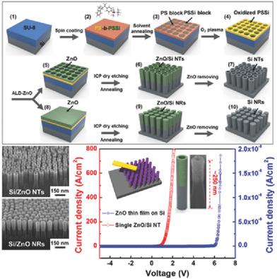
A novel and feasible methodology is developed to fabricate well‐ordered, freestanding 1D n‐ZnO/p‐Si nanotube (NT) and nanorod (NR) arrays via double‐patterning technology with block copolymer (BCP) self‐assembly, atomic layer deposition (ALD), and inductively coupled plasma (ICP) dry etching. To obtain the well‐ordered NT pattern, a self‐assembled, Si‐containing poly(styrene‐block‐4‐(tert‐butyldimethylsilyl)oxystyrene) BCP on an SU‐8/p‐Si wafer is employed as a template. After n‐ZnO deposition on the self‐assembled BCP template by ALD, an ICP etching process is performed to produce well‐defined, independent n‐ZnO/p‐Si NT arrays. The insights into the nanoarrays presented here are directly applicable to the fabrication of n‐ZnO/p‐Si NT/NR patterns and Si NT/NR patterns by precisely controlling the ALD cycles and ICP etching time. The electrical properties of a single n‐ZnO/p‐Si NT are measured by conductive atomic force microscopy, and the results show the typical rectifying behavior of a nanodiode with superior electrical properties. This simple and useful approach provides a very convenient route for fabricating high‐density nanodiode patterns. Additionally, the possibility of various applications is confirmed by simple analyses, including examinations of contact angle and reflectance. Furthermore, the wettability and antireflection properties can be controlled by changing the nanoarray morphology.
中文翻译:

使用嵌段共聚物模板和原子层沉积的圆形双图案平版印刷
通过使用嵌段共聚物(BCP)自组装,原子层沉积的双重图案技术,开发了一种新颖且可行的方法来制造有序,独立的一维n-ZnO / p-Si纳米管(NT)和纳米棒(NR)阵列(ALD)和电感耦合等离子体(ICP)干法蚀刻。为了获得井井有条的NT模式,需要自组装的含Si聚(苯乙烯嵌段-4-(叔)SU-8 / p-Si晶片上的[丁基丁基二甲基甲硅烷基)氧基苯乙烯)BCP被用作模板。通过ALD将n-ZnO沉积在自组装的BCP模板上后,将执行ICP蚀刻工艺以产生定义明确的独立n-ZnO / p-Si NT阵列。通过精确控制ALD循环和ICP刻蚀时间,此处介绍的纳米阵列的见解可直接应用于n-ZnO / p-Si NT / NR图案和Si NT / NR图案的制造。通过导电原子力显微镜测量单个n-ZnO / p-Si NT的电性能,结果表明具有优良电性能的纳米二极管的典型整流行为。这种简单而有用的方法为制造高密度纳米二极管图形提供了非常方便的途径。此外,通过简单的分析即可确定各种应用的可能性,包括检查接触角和反射率。此外,可通过改变纳米阵列的形态来控制润湿性和抗反射特性。
更新日期:2018-04-20
中文翻译:
使用嵌段共聚物模板和原子层沉积的圆形双图案平版印刷
通过使用嵌段共聚物(BCP)自组装,原子层沉积的双重图案技术,开发了一种新颖且可行的方法来制造有序,独立的一维n-ZnO / p-Si纳米管(NT)和纳米棒(NR)阵列(ALD)和电感耦合等离子体(ICP)干法蚀刻。为了获得井井有条的NT模式,需要自组装的含Si聚(苯乙烯嵌段-4-(叔)SU-8 / p-Si晶片上的[丁基丁基二甲基甲硅烷基)氧基苯乙烯)BCP被用作模板。通过ALD将n-ZnO沉积在自组装的BCP模板上后,将执行ICP蚀刻工艺以产生定义明确的独立n-ZnO / p-Si NT阵列。通过精确控制ALD循环和ICP刻蚀时间,此处介绍的纳米阵列的见解可直接应用于n-ZnO / p-Si NT / NR图案和Si NT / NR图案的制造。通过导电原子力显微镜测量单个n-ZnO / p-Si NT的电性能,结果表明具有优良电性能的纳米二极管的典型整流行为。这种简单而有用的方法为制造高密度纳米二极管图形提供了非常方便的途径。此外,通过简单的分析即可确定各种应用的可能性,包括检查接触角和反射率。此外,可通过改变纳米阵列的形态来控制润湿性和抗反射特性。


 京公网安备 11010802027423号