Our official English website, www.x-mol.net, welcomes your
feedback! (Note: you will need to create a separate account there.)
A technique for a nano-textured gapless microlens array using self-formation characteristics of anodic alumina†
Nanoscale ( IF 5.8 ) Pub Date : 2018-04-23 00:00:00 , DOI: 10.1039/c7nr07440a Yong Min Park 1, 2, 3, 4 , Woong Ki Jang 1, 2, 3, 4 , Tae Hwan Shin 1, 2, 3, 4 , Byeong Hee Kim 1, 2, 3, 4 , Young Ho Seo 1, 2, 3, 4
Nanoscale ( IF 5.8 ) Pub Date : 2018-04-23 00:00:00 , DOI: 10.1039/c7nr07440a Yong Min Park 1, 2, 3, 4 , Woong Ki Jang 1, 2, 3, 4 , Tae Hwan Shin 1, 2, 3, 4 , Byeong Hee Kim 1, 2, 3, 4 , Young Ho Seo 1, 2, 3, 4
Affiliation
|
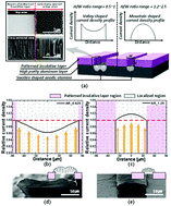
This paper presents a method to utilize the growth properties of anodic alumina possessing self-formation characteristics to fabricate a nano-textured microstructure and also introduces an application technique of the proposed method. The growth rate of anodic alumina, fabricated on aluminum surfaces, has a strong dependence on the intensity of the applied current density or electric field. The uniformity of the thickness of anodic alumina is determined by its electrical distribution characteristics. Accordingly, microscale structures can be fabricated using the growth rate deviation of anodic alumina. A patterned insulative layer is an important factor that determines the current density distribution property of a local region. A computational analysis and a verification experiment can verify this characteristic through the correlation between structural dimensional conditions and a cross-section of the fabricated anodic alumina. The anodic alumina fabricated by the verification experiment in this study had a swollen shape and a nano & micro complex structure, in which a nanoscale base pattern was formed on all bottom surface due to the process characteristics. Based on the advantages of the proposed process, evidenced by the reliability evaluation results, gapless microlens array (MLA) replication molds with nanostructured surfaces were fabricated to verify the applicability of the proposed technique to other fields. A patterned insulative layer with a cylindrical cavity and dimensional conditions was designed to induce the fabrication of lens-shaped anodic alumina. The anodic alumina fabricated by the long process was selectively etched out, and an additional process was conducted to fabricate a nanoporous structure having controlled dimensional conditions on the engraved gapless MLA surface. The textured aluminum surface was used as a replication mold for the imprinting process. The analysis of the fabrication results showed that the gapless MLA surface had a nanopillar structure. In addition, we investigated the reflection characteristics of the fabricated gapless N-MLA structure according to the incident light and verified the low reflectance of the gapless microlens. The results of this study affirmed that the proposed technique is applicable to various fields including those concerning optical devices.
中文翻译:

一种用于使用阳极氧化铝的自我形成特性的纳米纹理无间隙的微透镜阵列技术†
本文提出了一种利用具有自我形成特性的阳极氧化铝的生长特性来制备纳米织构微结构的方法,并介绍了该方法的应用技术。在铝表面上制造的阳极氧化铝的生长速率强烈依赖于所施加的电流密度或电场的强度。阳极氧化铝厚度的均匀性取决于其电分布特性。因此,可以使用阳极氧化铝的生长速率偏差来制造微尺度结构。图案化的绝缘层是确定局部区域的电流密度分布特性的重要因素。计算分析和验证实验可以通过结构尺寸条件与所制备的阳极氧化铝的横截面之间的相关性来验证该特性。通过本研究的验证实验制备的阳极氧化铝具有溶胀的形状和纳米微复合结构,其中由于工艺特性,在所有底表面上均形成了纳米级的基本图案。基于所提方法的优势,通过可靠性评估结果证明,制造了具有纳米结构表面的无间隙微透镜阵列(MLA)复制模具,以验证所提技术在其他领域的适用性。设计具有圆柱腔和尺寸条件的带图案的绝缘层,以诱导制造透镜状阳极氧化铝。选择性地蚀刻掉通过长工艺制造的阳极氧化铝,并进行了另一工艺以在雕刻的无间隙MLA表面上制造尺寸条件受控的纳米多孔结构。带纹理的铝表面用作压印过程的复制模具。对制造结果的分析表明,无间隙的MLA表面具有纳米柱结构。此外,我们根据入射光研究了制造的无间隙N-MLA结构的反射特性,并验证了无间隙微透镜的低反射率。这项研究的结果证实了所提出的技术适用于包括光学器件在内的各个领域。然后进行额外的工艺以在雕刻的无间隙MLA表面上制造尺寸条件受控的纳米多孔结构。带纹理的铝表面用作压印过程的复制模具。对制造结果的分析表明,无间隙的MLA表面具有纳米柱结构。此外,我们根据入射光研究了制造的无间隙N-MLA结构的反射特性,并验证了无间隙微透镜的低反射率。这项研究的结果证实了所提出的技术适用于包括光学器件在内的各个领域。然后进行额外的工艺以在雕刻的无间隙MLA表面上制造尺寸条件受控的纳米多孔结构。带纹理的铝表面用作压印过程的复制模具。对制造结果的分析表明,无间隙的MLA表面具有纳米柱结构。此外,我们根据入射光研究了制造的无间隙N-MLA结构的反射特性,并验证了无间隙微透镜的低反射率。这项研究的结果证实了所提出的技术适用于包括光学器件在内的各个领域。带纹理的铝表面用作压印过程的复制模具。对制造结果的分析表明,无间隙的MLA表面具有纳米柱结构。此外,我们根据入射光研究了制造的无间隙N-MLA结构的反射特性,并验证了无间隙微透镜的低反射率。这项研究的结果证实了所提出的技术适用于包括光学器件在内的各个领域。带纹理的铝表面用作压印过程的复制模具。对制造结果的分析表明,无间隙的MLA表面具有纳米柱结构。此外,我们根据入射光研究了制造的无间隙N-MLA结构的反射特性,并验证了无间隙微透镜的低反射率。这项研究的结果证实了所提出的技术适用于包括光学器件在内的各个领域。
更新日期:2018-04-23
中文翻译:
一种用于使用阳极氧化铝的自我形成特性的纳米纹理无间隙的微透镜阵列技术†
本文提出了一种利用具有自我形成特性的阳极氧化铝的生长特性来制备纳米织构微结构的方法,并介绍了该方法的应用技术。在铝表面上制造的阳极氧化铝的生长速率强烈依赖于所施加的电流密度或电场的强度。阳极氧化铝厚度的均匀性取决于其电分布特性。因此,可以使用阳极氧化铝的生长速率偏差来制造微尺度结构。图案化的绝缘层是确定局部区域的电流密度分布特性的重要因素。计算分析和验证实验可以通过结构尺寸条件与所制备的阳极氧化铝的横截面之间的相关性来验证该特性。通过本研究的验证实验制备的阳极氧化铝具有溶胀的形状和纳米微复合结构,其中由于工艺特性,在所有底表面上均形成了纳米级的基本图案。基于所提方法的优势,通过可靠性评估结果证明,制造了具有纳米结构表面的无间隙微透镜阵列(MLA)复制模具,以验证所提技术在其他领域的适用性。设计具有圆柱腔和尺寸条件的带图案的绝缘层,以诱导制造透镜状阳极氧化铝。选择性地蚀刻掉通过长工艺制造的阳极氧化铝,并进行了另一工艺以在雕刻的无间隙MLA表面上制造尺寸条件受控的纳米多孔结构。带纹理的铝表面用作压印过程的复制模具。对制造结果的分析表明,无间隙的MLA表面具有纳米柱结构。此外,我们根据入射光研究了制造的无间隙N-MLA结构的反射特性,并验证了无间隙微透镜的低反射率。这项研究的结果证实了所提出的技术适用于包括光学器件在内的各个领域。然后进行额外的工艺以在雕刻的无间隙MLA表面上制造尺寸条件受控的纳米多孔结构。带纹理的铝表面用作压印过程的复制模具。对制造结果的分析表明,无间隙的MLA表面具有纳米柱结构。此外,我们根据入射光研究了制造的无间隙N-MLA结构的反射特性,并验证了无间隙微透镜的低反射率。这项研究的结果证实了所提出的技术适用于包括光学器件在内的各个领域。然后进行额外的工艺以在雕刻的无间隙MLA表面上制造尺寸条件受控的纳米多孔结构。带纹理的铝表面用作压印过程的复制模具。对制造结果的分析表明,无间隙的MLA表面具有纳米柱结构。此外,我们根据入射光研究了制造的无间隙N-MLA结构的反射特性,并验证了无间隙微透镜的低反射率。这项研究的结果证实了所提出的技术适用于包括光学器件在内的各个领域。带纹理的铝表面用作压印过程的复制模具。对制造结果的分析表明,无间隙的MLA表面具有纳米柱结构。此外,我们根据入射光研究了制造的无间隙N-MLA结构的反射特性,并验证了无间隙微透镜的低反射率。这项研究的结果证实了所提出的技术适用于包括光学器件在内的各个领域。带纹理的铝表面用作压印过程的复制模具。对制造结果的分析表明,无间隙的MLA表面具有纳米柱结构。此外,我们根据入射光研究了制造的无间隙N-MLA结构的反射特性,并验证了无间隙微透镜的低反射率。这项研究的结果证实了所提出的技术适用于包括光学器件在内的各个领域。


 京公网安备 11010802027423号