当前位置:
X-MOL 学术
›
J. Mater. Chem. A
›
论文详情
Our official English website, www.x-mol.net, welcomes your feedback! (Note: you will need to create a separate account there.)
Two-dimensional GeAs with a visible range band gap†
Journal of Materials Chemistry A ( IF 11.9 ) Pub Date : 2018-04-19 00:00:00 , DOI: 10.1039/c8ta02676a Chan Su Jung 1, 2, 3, 4 , Doyeon Kim 1, 2, 3, 4 , Seunghwan Cha 4, 5, 6, 7 , Yoon Myung 4, 8, 9, 10 , Fazel Shojaei 4, 11, 12, 13 , Hafiz Ghulam Abbas 4, 14, 15 , Jung Ah Lee 1, 2, 3, 4 , Eun Hee Cha 4, 5, 6, 7 , Jeunghee Park 1, 2, 3, 4 , Hong Seok Kang 4, 13, 16, 17
Journal of Materials Chemistry A ( IF 11.9 ) Pub Date : 2018-04-19 00:00:00 , DOI: 10.1039/c8ta02676a Chan Su Jung 1, 2, 3, 4 , Doyeon Kim 1, 2, 3, 4 , Seunghwan Cha 4, 5, 6, 7 , Yoon Myung 4, 8, 9, 10 , Fazel Shojaei 4, 11, 12, 13 , Hafiz Ghulam Abbas 4, 14, 15 , Jung Ah Lee 1, 2, 3, 4 , Eun Hee Cha 4, 5, 6, 7 , Jeunghee Park 1, 2, 3, 4 , Hong Seok Kang 4, 13, 16, 17
Affiliation
|
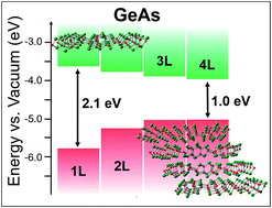
Two-dimensional (2D) layered structures have recently drawn worldwide attention because of their intriguing optical and electrical properties. In this study, we prepared GeAs nanosheets as a new 2D material by a liquid-phase exfoliation method. The few-layered nanosheets had a band gap close to 2.1 eV, which is significantly higher (by about 1.5 eV) compared to the bulk. The value of 2.1 eV is in excellent agreement with that for the monolayer obtained from first-principles (HSE-06) calculations; mono-, bi-, tri-, and tetra-layers have remarkable direct or quasi-direct band gaps of 2.125, 1.339, 1.112, and 1.017 eV, respectively. The electrical properties of individual GeAs nanosheets were measured to reveal their 2D carrier transport behaviors. We also observed stable and large photocurrents, indicating potential application in high-performance optoelectronic nanodevices. The few-layered GeAs nanosheets deposited on n-type Si nanowire arrays showed promising photoelectrochemical water splitting under visible light irradiation. Band alignment based on the calculated band edge positions suggested a buildup of the space charge region in the p-GeAs/n-Si heterojunction, as well as the band bending of n-Si at the electrolyte interface.
中文翻译:

具有可见范围带隙的二维GeAs †
二维(2D)分层结构由于其吸引人的光学和电学特性,最近引起了全世界的关注。在这项研究中,我们通过液相剥离法将GeAs纳米片制备为一种新型2D材料。几层纳米片的带隙接近2.1 eV,与整体相比明显更高(约1.5 eV)。2.1 eV的值与从第一性原理(HSE-06)计算得出的单层的值非常一致;单层,双层,三层和四层具有明显的直接或准直接带隙,分别为2.125、1.339、1.112和1.017 eV。测量各个GeAs纳米片的电性能,以揭示其2D载流子传输行为。我们还观察到稳定且较大的光电流,表明在高性能光电纳米器件中的潜在应用。沉积在n型Si纳米线阵列上的几层GeAs纳米片在可见光照射下显示出有希望的光电化学水分解。基于计算的能带边缘位置的能带对准表明,p-GeAs / n-Si异质结中空间电荷区域的积累,以及电解质界面处n-Si的能带弯曲。
更新日期:2018-04-19
中文翻译:
具有可见范围带隙的二维GeAs †
二维(2D)分层结构由于其吸引人的光学和电学特性,最近引起了全世界的关注。在这项研究中,我们通过液相剥离法将GeAs纳米片制备为一种新型2D材料。几层纳米片的带隙接近2.1 eV,与整体相比明显更高(约1.5 eV)。2.1 eV的值与从第一性原理(HSE-06)计算得出的单层的值非常一致;单层,双层,三层和四层具有明显的直接或准直接带隙,分别为2.125、1.339、1.112和1.017 eV。测量各个GeAs纳米片的电性能,以揭示其2D载流子传输行为。我们还观察到稳定且较大的光电流,表明在高性能光电纳米器件中的潜在应用。沉积在n型Si纳米线阵列上的几层GeAs纳米片在可见光照射下显示出有希望的光电化学水分解。基于计算的能带边缘位置的能带对准表明,p-GeAs / n-Si异质结中空间电荷区域的积累,以及电解质界面处n-Si的能带弯曲。


 京公网安备 11010802027423号