Our official English website, www.x-mol.net, welcomes your
feedback! (Note: you will need to create a separate account there.)
Single-crystalline perovskite wafers with a Cr blocking layer for broad and stable light detection in a harsh environment†
RSC Advances ( IF 3.9 ) Pub Date : 2018-04-19 00:00:00 , DOI: 10.1039/c8ra02709a Qian Wang 1 , Dongliang Bai 1 , Zhiwen Jin 1 , Shengzhong Frank Liu 1, 2
RSC Advances ( IF 3.9 ) Pub Date : 2018-04-19 00:00:00 , DOI: 10.1039/c8ra02709a Qian Wang 1 , Dongliang Bai 1 , Zhiwen Jin 1 , Shengzhong Frank Liu 1, 2
Affiliation
|
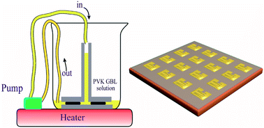
Herein, ultrathin (∼35 μm) CH3NH3PbI3 (MAPbI3) single-crystalline wafers have been successfully prepared by using an appropriate geometry-regulated dynamic-flow reaction system. The measurement results proved that the obtained wafers have high crystallinity, and showed broad light absorption from ultraviolet to near infrared (850 nm) which can be attributed to the indirect bandgap. Straight after, such an MAPbI3 wafer was used to fabricate high-quality photodetectors (PDs). On account of its faster carrier transport and significantly reduced defect density, the device exhibits a high photoresponse (R) of 5 A/W and short on/off response (0.039 s/0.017 s). Interestingly, by introducing a Cr interlayer between the MAPbI3 wafer and the Au electrode to avoid the migration of Au, the PD shows nearly no degradation when it works at 200 °C. Furthermore, the device performance shows very little degradation over the course of 60 days of storage under ambient conditions owing to its lack of grain boundaries. We believe the strategy reported here is very promising for achieving broad photodetection in a harsh environment.
中文翻译:

具有 Cr 阻挡层的单晶钙钛矿晶圆,可在恶劣环境下实现广泛且稳定的光检测†
在此,通过使用适当的几何调节动态流反应系统成功制备了超薄(~35 μm)CH 3 NH 3 PbI 3 (MAPbI 3 )单晶晶片。测量结果证明,所获得的晶片具有高结晶度,并且表现出从紫外到近红外(850 nm)的宽广的光吸收,这可归因于间接带隙。紧接着,这样的 MAPbI 3晶圆就被用来制造高质量的光电探测器 (PD)。由于其更快的载流子传输和显着降低的缺陷密度,该器件表现出5 A/W 的高光响应 ( R ) 和短的开/关响应 (0.039 s/0.017 s)。有趣的是,通过在MAPbI 3晶圆和Au电极之间引入Cr中间层来避免Au的迁移,PD在200℃下工作时几乎没有表现出退化。此外,由于没有晶界,在环境条件下 60 天的存储过程中,器件性能几乎没有下降。我们相信这里报告的策略对于在恶劣环境中实现广泛的光电检测非常有希望。
更新日期:2018-04-19
中文翻译:
具有 Cr 阻挡层的单晶钙钛矿晶圆,可在恶劣环境下实现广泛且稳定的光检测†
在此,通过使用适当的几何调节动态流反应系统成功制备了超薄(~35 μm)CH 3 NH 3 PbI 3 (MAPbI 3 )单晶晶片。测量结果证明,所获得的晶片具有高结晶度,并且表现出从紫外到近红外(850 nm)的宽广的光吸收,这可归因于间接带隙。紧接着,这样的 MAPbI 3晶圆就被用来制造高质量的光电探测器 (PD)。由于其更快的载流子传输和显着降低的缺陷密度,该器件表现出5 A/W 的高光响应 ( R ) 和短的开/关响应 (0.039 s/0.017 s)。有趣的是,通过在MAPbI 3晶圆和Au电极之间引入Cr中间层来避免Au的迁移,PD在200℃下工作时几乎没有表现出退化。此外,由于没有晶界,在环境条件下 60 天的存储过程中,器件性能几乎没有下降。我们相信这里报告的策略对于在恶劣环境中实现广泛的光电检测非常有希望。


 京公网安备 11010802027423号