Our official English website, www.x-mol.net, welcomes your
feedback! (Note: you will need to create a separate account there.)
Pulse laser-induced size-controllable and symmetrical ordering of single-crystal Si islands†
Nanoscale ( IF 5.8 ) Pub Date : 2018-04-03 00:00:00 , DOI: 10.1039/c8nr00210j Dongfeng Qi 1, 2, 3, 4, 5 , Shiwei Tang 1, 2, 3, 4, 5 , Letian Wang 6, 7, 8, 9, 10 , Shixun Dai 1, 2, 3, 4, 5 , Xiang Shen 1, 2, 3, 4, 5 , Chen Wang 11, 12, 13, 14 , Songyan Chen 5, 13, 15, 16
Nanoscale ( IF 5.8 ) Pub Date : 2018-04-03 00:00:00 , DOI: 10.1039/c8nr00210j Dongfeng Qi 1, 2, 3, 4, 5 , Shiwei Tang 1, 2, 3, 4, 5 , Letian Wang 6, 7, 8, 9, 10 , Shixun Dai 1, 2, 3, 4, 5 , Xiang Shen 1, 2, 3, 4, 5 , Chen Wang 11, 12, 13, 14 , Songyan Chen 5, 13, 15, 16
Affiliation
|
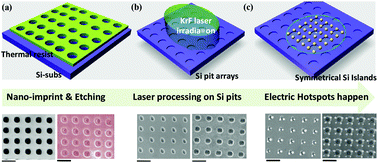
Optically electric- and magnetic resonance-induced dielectric nanostructures have garnered significant attention due to applications as tunable electronic and optoelectronic device. In this letter, we describe an ultrafast and large-area method to construct symmetrical and single-crystal Si island structures directly on Si substrates by a pulse laser dewetting method. The tunable surface electric field intensity distribution could convert the stochastic dewetting process into a deterministic process (classical dipole mode and Mie resonance dipole mode) on predefined Si pit arrays via laser dewetting. Under this condition, these pre-patterned Si substrate structures not only induced high spatial ordering of islands, but also improved their size uniformity. By adjusting the laser fluence, the diameter of the single-crystal Si islands could be selected in the range 41.7–147.1 nm.
中文翻译:

脉冲激光诱导的单晶硅岛的尺寸可控和对称有序†
由于作为可调谐电子和光电子器件的应用,由光学的电和磁共振引起的介电纳米结构已经引起了广泛的关注。在这封信中,我们描述了一种通过脉冲激光去湿法在硅衬底上直接构造对称且单晶硅岛结构的超快速大面积方法。可调节的表面电场强度分布可以通过以下方法将预定义的硅凹坑阵列上的随机去湿过程转换为确定性过程(经典偶极子模式和Mie共振偶极子模式)。激光去湿。在这种条件下,这些预先构图的硅衬底结构不仅引起岛的高空间有序性,而且提高了其尺寸均匀性。通过调整激光能量密度,可以在41.7–147.1 nm的范围内选择单晶硅岛的直径。
更新日期:2018-04-03
中文翻译:
脉冲激光诱导的单晶硅岛的尺寸可控和对称有序†
由于作为可调谐电子和光电子器件的应用,由光学的电和磁共振引起的介电纳米结构已经引起了广泛的关注。在这封信中,我们描述了一种通过脉冲激光去湿法在硅衬底上直接构造对称且单晶硅岛结构的超快速大面积方法。可调节的表面电场强度分布可以通过以下方法将预定义的硅凹坑阵列上的随机去湿过程转换为确定性过程(经典偶极子模式和Mie共振偶极子模式)。激光去湿。在这种条件下,这些预先构图的硅衬底结构不仅引起岛的高空间有序性,而且提高了其尺寸均匀性。通过调整激光能量密度,可以在41.7–147.1 nm的范围内选择单晶硅岛的直径。


 京公网安备 11010802027423号