当前位置:
X-MOL 学术
›
Chem. Mater.
›
论文详情
Our official English website, www.x-mol.net, welcomes your
feedback! (Note: you will need to create a separate account there.)
Shape-, Size-, and Composition-Controlled Thallium Lead Halide Perovskite Nanowires and Nanocrystals with Tunable Band Gaps
Chemistry of Materials ( IF 7.2 ) Pub Date : 2018-04-03 00:00:00 , DOI: 10.1021/acs.chemmater.8b00421 Parth Vashishtha 1 , Dani Z. Metin 2 , Matthew E. Cryer 1 , Kai Chen 1 , Justin M. Hodgkiss 1 , Nicola Gaston 2 , Jonathan E. Halpert 1, 3
Chemistry of Materials ( IF 7.2 ) Pub Date : 2018-04-03 00:00:00 , DOI: 10.1021/acs.chemmater.8b00421 Parth Vashishtha 1 , Dani Z. Metin 2 , Matthew E. Cryer 1 , Kai Chen 1 , Justin M. Hodgkiss 1 , Nicola Gaston 2 , Jonathan E. Halpert 1, 3
Affiliation
|
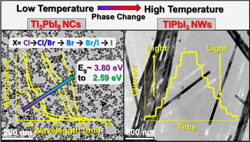
Perovskite nanocrystals have shown themselves to be useful for both absorption- and emission-based applications, including solar cells, photodetectors, and LEDs. Here we present a new class of size-, composition-, and shape-tunable nanocrystals made from Tl3PbX5 (X= Cl, Br, I). These can be synthesized via colloidal methods to produce faceted spheroidal nanocrystals, and perovskite TlPbI3 nanowires. Crystal structures for the orthorhombic and tetragonal phase materials, for both pure and mixed halide species, are compared to the literature and also calculated from first-principles in VASP. We show the ability to tune the band gap by halide substitution to create materials that can absorb strongly between 250 and 450 nm. In addition, we show evidence of the confinement effect in pure halide Tl3PbBr5 nanocrystals suggesting size-tuning is possible as well. By tuning the band gap we can create materials with specific absorption spectra suitable for photodetection that display conduction and photoresponse properties similar to previously observed perovskite nanocrystals. We also observe weak emission consistent with indirect band-gap materials. Finally, we are able to demonstrate shape control in these materials, to give some insight into observable phase changes with varying reaction conditions, and to demonstrate the utility of the TlPbI3 perovskite nanowires as wide-band-gap photoconductors. These novel perovskite nanocrystalline materials can be expected to find applications in photodetectors, X-ray detectors, and piezoelectrics.
中文翻译:

具有可调带隙的形状,尺寸和成分控制的hall卤化钙铅钙钛矿纳米线和纳米晶体
钙钛矿纳米晶体已显示出可用于基于吸收和发射的应用,包括太阳能电池,光电探测器和LED。在这里,我们介绍了由Tl 3 PbX 5(X = Cl,Br,I)制成的一类尺寸,组成和形状可调的纳米晶体。这些可以通过胶体方法合成以产生多面球形纳米晶体和钙钛矿TlPbI 3。纳米线。将正交和四方相材料的晶体结构(无论是纯卤化物还是混合卤化物)与文献进行比较,并从VASP中的第一性原理进行计算。我们展示了通过卤化物取代来调节能带隙的能力,以创建可以在250至450 nm之间强烈吸收的材料。此外,我们显示了纯卤化物Tl 3 PbBr 5中的限制作用证据。暗示尺寸调整的纳米晶体也是可能的。通过调整带隙,我们可以创建具有特定吸收光谱的材料,这些材料适用于光检测,显示出类似于先前观察到的钙钛矿纳米晶体的导电和光响应特性。我们还观察到与间接带隙材料一致的弱发射。最后,我们能够证明这些材料的形状控制,对可观察到的随着变化的反应条件而发生的相变有所了解,并证明TlPbI 3钙钛矿纳米线作为宽带隙光电导体的实用性。这些新颖的钙钛矿纳米晶体材料有望在光电探测器,X射线探测器和压电器件中找到应用。
更新日期:2018-04-03
中文翻译:
具有可调带隙的形状,尺寸和成分控制的hall卤化钙铅钙钛矿纳米线和纳米晶体
钙钛矿纳米晶体已显示出可用于基于吸收和发射的应用,包括太阳能电池,光电探测器和LED。在这里,我们介绍了由Tl 3 PbX 5(X = Cl,Br,I)制成的一类尺寸,组成和形状可调的纳米晶体。这些可以通过胶体方法合成以产生多面球形纳米晶体和钙钛矿TlPbI 3。纳米线。将正交和四方相材料的晶体结构(无论是纯卤化物还是混合卤化物)与文献进行比较,并从VASP中的第一性原理进行计算。我们展示了通过卤化物取代来调节能带隙的能力,以创建可以在250至450 nm之间强烈吸收的材料。此外,我们显示了纯卤化物Tl 3 PbBr 5中的限制作用证据。暗示尺寸调整的纳米晶体也是可能的。通过调整带隙,我们可以创建具有特定吸收光谱的材料,这些材料适用于光检测,显示出类似于先前观察到的钙钛矿纳米晶体的导电和光响应特性。我们还观察到与间接带隙材料一致的弱发射。最后,我们能够证明这些材料的形状控制,对可观察到的随着变化的反应条件而发生的相变有所了解,并证明TlPbI 3钙钛矿纳米线作为宽带隙光电导体的实用性。这些新颖的钙钛矿纳米晶体材料有望在光电探测器,X射线探测器和压电器件中找到应用。


 京公网安备 11010802027423号