Our official English website, www.x-mol.net, welcomes your
feedback! (Note: you will need to create a separate account there.)
Intra- and inter-nanocrystal charge transport in nanocrystal films
Nanoscale ( IF 5.8 ) Pub Date : 2018-03-26 00:00:00 , DOI: 10.1039/c8nr00250a Willi Aigner 1, 2, 3, 4 , Oliver Bienek 1, 2, 3, 4 , Bruno P. Falcão 5, 6, 7, 8 , Safwan U. Ahmed 1, 2, 3, 4 , Hartmut Wiggers 4, 9, 10, 11, 12 , Martin Stutzmann 1, 2, 3, 4 , Rui N. Pereira 1, 2, 3, 4, 5
Nanoscale ( IF 5.8 ) Pub Date : 2018-03-26 00:00:00 , DOI: 10.1039/c8nr00250a Willi Aigner 1, 2, 3, 4 , Oliver Bienek 1, 2, 3, 4 , Bruno P. Falcão 5, 6, 7, 8 , Safwan U. Ahmed 1, 2, 3, 4 , Hartmut Wiggers 4, 9, 10, 11, 12 , Martin Stutzmann 1, 2, 3, 4 , Rui N. Pereira 1, 2, 3, 4, 5
Affiliation
|
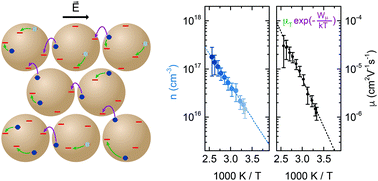
The exploitation of semiconductor nanocrystal (NC) films in novel electronic and optoelectronic applications requires a better understanding of charge transport in these systems. Here, we develop a model of charge transport in NC films, based on a generalization of the concept of transport energy level ET to nanocrystal assemblies, which considers both intra- and inter-NC charge transfer processes. We conclude that the role played by each of these processes can be probed from temperature-dependent measurements of charge carrier density n and mobility μ in the same films. The model also enables the determination of the position of the Fermi energy level EF with respect to ET, an important parameter of charge transport in semiconductor materials, from the temperature dependence of n. Moreover, we provide support to an essentially temperature-independent intra-NC charge carrier mobility, considered in the transport level concept, and consequently the frequently observed temperature dependence of the overall mobility μ in NC films results from a temperature variation of the inter-NC charge transport processes. Importantly, we also conclude that the temperature dependence of conductivity in NC films should result in general from a combination of temperature variations of both n and μ. By applying the model to solution-processed Si NC films, we conclude that transport within each NC is similar to that in amorphous Si (a-Si), with charges hopping along band tail states located below the conduction band edge. For Si NCs, we obtain values of ET − EF of ∼0.25 eV. The overall mobility μ in Si NC films is significantly further reduced with respect to that typically found in a-Si due to the additional transport constraints imposed by inter-NC transfer processes inherent to a nanoparticulate film. Our model accounting for inter- and intra-NC charge transport processes provides a simple and more general description of charge transport that can be broadly applied to films of semiconductor NCs.
中文翻译:

纳米晶体薄膜中纳米晶体内部和内部的电荷传输
在新颖的电子和光电应用中对半导体纳米晶体(NC)膜的开发要求对这些系统中的电荷传输有更好的了解。在这里,我们基于到纳米晶体组件的传输能级E T的概念的概括,开发了NC薄膜中的电荷传输模型,该模型考虑了NC内部和内部的电荷转移过程。我们得出结论,可以从同一膜中电荷载流子密度n和迁移率μ的温度相关测量中探究这些过程中每个过程所起的作用。该模型还可以确定费米能级E F相对于E T的位置n是温度与温度的关系,它是半导体材料中电荷传输的重要参数。此外,我们为在运输水平概念中考虑的,与温度基本无关的内部NC载流子迁移率提供了支持,因此,经常观察到的NC膜中总迁移率μ的温度依赖性是由NC间的温度变化引起的电荷运输过程。重要的是,我们还得出结论,通常应该由n和μ的温度变化共同导致NC膜中电导率的温度依赖性。。通过将该模型应用于固溶处理的Si NC薄膜,我们得出的结论是,每个NC中的迁移与非晶Si(a-Si)中的迁移相似,电荷沿着位于导带边缘以下的带尾态跳跃。对于Si NC,我们获得的E T - E F值为0.25 eV。相对于通常在a-Si中发现的迁移率μ,由于纳米颗粒膜固有的NC间转移过程带来的附加传输限制,Si NC膜中的总体迁移率μ大大降低。我们考虑到NC内部和内部NC电荷传输过程的模型提供了一个简单且更笼统的电荷传输描述,可以广泛地应用于半导体NC的薄膜。
更新日期:2018-03-26
中文翻译:
纳米晶体薄膜中纳米晶体内部和内部的电荷传输
在新颖的电子和光电应用中对半导体纳米晶体(NC)膜的开发要求对这些系统中的电荷传输有更好的了解。在这里,我们基于到纳米晶体组件的传输能级E T的概念的概括,开发了NC薄膜中的电荷传输模型,该模型考虑了NC内部和内部的电荷转移过程。我们得出结论,可以从同一膜中电荷载流子密度n和迁移率μ的温度相关测量中探究这些过程中每个过程所起的作用。该模型还可以确定费米能级E F相对于E T的位置n是温度与温度的关系,它是半导体材料中电荷传输的重要参数。此外,我们为在运输水平概念中考虑的,与温度基本无关的内部NC载流子迁移率提供了支持,因此,经常观察到的NC膜中总迁移率μ的温度依赖性是由NC间的温度变化引起的电荷运输过程。重要的是,我们还得出结论,通常应该由n和μ的温度变化共同导致NC膜中电导率的温度依赖性。。通过将该模型应用于固溶处理的Si NC薄膜,我们得出的结论是,每个NC中的迁移与非晶Si(a-Si)中的迁移相似,电荷沿着位于导带边缘以下的带尾态跳跃。对于Si NC,我们获得的E T - E F值为0.25 eV。相对于通常在a-Si中发现的迁移率μ,由于纳米颗粒膜固有的NC间转移过程带来的附加传输限制,Si NC膜中的总体迁移率μ大大降低。我们考虑到NC内部和内部NC电荷传输过程的模型提供了一个简单且更笼统的电荷传输描述,可以广泛地应用于半导体NC的薄膜。


 京公网安备 11010802027423号