Our official English website, www.x-mol.net, welcomes your
feedback! (Note: you will need to create a separate account there.)
Non-destructive characterization of extended crystalline defects in confined semiconductor device structures†
Nanoscale ( IF 5.8 ) Pub Date : 2018-03-26 00:00:00 , DOI: 10.1039/c8nr00186c Andreas Schulze 1, 2, 3 , Libor Strakos 4, 5, 6 , Tomas Vystavel 4, 5, 6 , Roger Loo 1, 2, 3 , Antoine Pacco 1, 2, 3 , Nadine Collaert 1, 2, 3 , Wilfried Vandervorst 1, 2, 3, 7, 8 , Matty Caymax 1, 2, 3
Nanoscale ( IF 5.8 ) Pub Date : 2018-03-26 00:00:00 , DOI: 10.1039/c8nr00186c Andreas Schulze 1, 2, 3 , Libor Strakos 4, 5, 6 , Tomas Vystavel 4, 5, 6 , Roger Loo 1, 2, 3 , Antoine Pacco 1, 2, 3 , Nadine Collaert 1, 2, 3 , Wilfried Vandervorst 1, 2, 3, 7, 8 , Matty Caymax 1, 2, 3
Affiliation
|
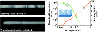
Semiconductor heterostructures are at the heart of most nanoelectronic and photonic devices such as advanced transistors, lasers, light emitting diodes, optical modulators and photo-detectors. However, the performance and reliability of the respective devices are often limited by the presence of crystalline defects which arise from plastic relaxation of misfit strain present in these heterogeneous systems. To date, characterizing the nature and distribution of such defects in 3D nanoscale devices precisely and non-destructively remains a critical metrology challenge. In this paper we demonstrate that electron channeling contrast imaging (ECCI) is capable of analyzing individual dislocations and stacking faults in confined 3D nanostructures, thereby fulfilling the aforementioned requirements. For this purpose we imaged the intensity of electrons backscattered from the sample under test under controlled diffraction conditions using a scanning electron microscope (SEM). In contrast to transmission electron microscopy (TEM) analysis, no electron transparent specimens need to be prepared. This enables a significant reduction of the detection limit (i.e. lowest defect density that can be assessed) as our approach facilitates the analysis of large sampling volumes, thereby providing excellent statistics. We applied the methodology to SiGe nanostructures grown by selective area epitaxy to study in detail how the nature and distribution of crystalline defects are affected by the dimensions of the structure. By comparing our observations with the results obtained using X-ray diffraction, TEM and chemical defect etching, we could verify the validity of the method. Our findings firmly establish that ECCI must be considered the method of choice for analyzing the crystalline quality of 3D semiconductor heterostructures with excellent precision even at low defect densities. As such, the technique aids in better understanding of strain relaxation and defect formation mechanisms at the nanoscale and, moreover, facilitates the development and fabrication of next generation nanoelectronic and photonic devices.
中文翻译:

受限半导体器件结构中扩展的晶体缺陷的无损表征†
半导体异质结构是大多数纳米电子和光子设备(如高级晶体管,激光器,发光二极管,光学调制器和光电探测器)的核心。但是,各个器件的性能和可靠性通常受到结晶缺陷的限制,这些缺陷是由这些异质系统中存在的失配应变的塑性松弛引起的。迄今为止,准确无损地表征3D纳米级器件中此类缺陷的性质和分布仍然是关键的计量挑战。在本文中,我们证明了电子通道对比成像(ECCI)能够分析受限3D纳米结构中的单个位错和堆叠缺陷,从而满足上述要求。为此,我们使用扫描电子显微镜(SEM)对在受控衍射条件下从被测样品中反向散射的电子的强度进行了成像。与透射电子显微镜(TEM)分析相比,无需准备电子透明样品。这样可以大大降低检测限(IE可以评估的最低缺陷密度),因为我们的方法有助于分析大样本量,从而提供出色的统计数据。我们将该方法应用于通过选择性区域外延生长的SiGe纳米结构,以详细研究晶体缺陷的性质和分布如何受到结构尺寸的影响。通过将我们的观察结果与使用X射线衍射,TEM和化学缺陷蚀刻获得的结果进行比较,我们可以验证该方法的有效性。我们的发现坚定地证明,即使在低缺陷密度下,ECCI也必须被视为分析3D半导体异质结构的晶体质量的首选方法。因此,该技术有助于更好地了解纳米级的应变松弛和缺陷形成机理,并且
更新日期:2018-03-26
中文翻译:
受限半导体器件结构中扩展的晶体缺陷的无损表征†
半导体异质结构是大多数纳米电子和光子设备(如高级晶体管,激光器,发光二极管,光学调制器和光电探测器)的核心。但是,各个器件的性能和可靠性通常受到结晶缺陷的限制,这些缺陷是由这些异质系统中存在的失配应变的塑性松弛引起的。迄今为止,准确无损地表征3D纳米级器件中此类缺陷的性质和分布仍然是关键的计量挑战。在本文中,我们证明了电子通道对比成像(ECCI)能够分析受限3D纳米结构中的单个位错和堆叠缺陷,从而满足上述要求。为此,我们使用扫描电子显微镜(SEM)对在受控衍射条件下从被测样品中反向散射的电子的强度进行了成像。与透射电子显微镜(TEM)分析相比,无需准备电子透明样品。这样可以大大降低检测限(IE可以评估的最低缺陷密度),因为我们的方法有助于分析大样本量,从而提供出色的统计数据。我们将该方法应用于通过选择性区域外延生长的SiGe纳米结构,以详细研究晶体缺陷的性质和分布如何受到结构尺寸的影响。通过将我们的观察结果与使用X射线衍射,TEM和化学缺陷蚀刻获得的结果进行比较,我们可以验证该方法的有效性。我们的发现坚定地证明,即使在低缺陷密度下,ECCI也必须被视为分析3D半导体异质结构的晶体质量的首选方法。因此,该技术有助于更好地了解纳米级的应变松弛和缺陷形成机理,并且


 京公网安备 11010802027423号