当前位置:
X-MOL 学术
›
Adv. Electron. Mater.
›
论文详情
Our official English website, www.x-mol.net, welcomes your
feedback! (Note: you will need to create a separate account there.)
Dimensional Crossover Transport Induced by Substitutional Atomic Doping in SnSe2
Advanced Electronic Materials ( IF 5.3 ) Pub Date : 2018-03-13 , DOI: 10.1002/aelm.201700563 Suyoun Lee 1, 2 , Young Tack Lee 3 , Seong Gon Park 4 , Kyu Hyoung Lee 5 , Sung Wng Kim 6 , Do Kyung Hwang 2, 7 , Kimoon Lee 4
Advanced Electronic Materials ( IF 5.3 ) Pub Date : 2018-03-13 , DOI: 10.1002/aelm.201700563 Suyoun Lee 1, 2 , Young Tack Lee 3 , Seong Gon Park 4 , Kyu Hyoung Lee 5 , Sung Wng Kim 6 , Do Kyung Hwang 2, 7 , Kimoon Lee 4
Affiliation
|
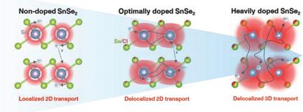
Substitutional atomic doping is one of the most convenient and precise routes to modulate semiconducting material properties. Although two‐dimensional (2D) layered transition metal dichalcogenides (TMDs) are of great interest as a prominent semiconducting material due to their unique physical/chemical properties, such a practical atomic doping is still rare, possibly due to the intrinsic localization nature of conduction paths based on d‐band states. Here, using single‐crystalline Cl‐doped SnSe2, the dimensional crossover in carrier transport accompanied by semiconductor‐to‐metal transition is reported. Nondoped SnSe2 shows semiconducting transport behavior dominated by 2D variable range hopping conduction, exhibiting relatively strong localization of carriers at low‐temperature regions. Moderately electron‐doped SnSe2 by substitution on Se with higher valent Cl exhibits superior electrical conductivity even than the heavily doped one owing to the higher electron mobility of the former (167 cm2 V−1 s−1 at 2 K). Combined with Raman spectra, temperature dependence of mobility clearly evidences the effective screening of homopolar optical mode phonon compared to typical TMD materials. Detailed characterizations with magnetoresistance behaviors finally demonstrate that the suppression of both homopolar optical mode phonon and carrier localization as retaining low‐dimensionality is key for high mobility conduction in electron‐doped SnSe2.
中文翻译:

SnSe2中取代原子掺杂引起的尺寸交叉传输。
替代原子掺杂是调节半导体材料性能的最方便,最精确的途径之一。尽管二维(2D)层状过渡金属二硫化碳(TMD)由于其独特的物理/化学性质而作为一种重要的半导体材料引起了人们的极大兴趣,但这种实际的原子掺杂仍然很少见,这可能是由于导电的固有局限性基于d波段状态的路径。在这里,使用单晶Cl掺杂的SnSe 2,报告了载流子传输中伴随着半导体到金属跃迁的尺寸交叉。非掺杂锡硒2显示了以2D变程跳变传导为主的半导体传输行为,在低温区域表现出了相对较强的载流子定位。适度电子掺杂位SnSe 2由硒取代成更高价的氯表现出优良的导电性,甚至比重由于前者(167厘米的较高电子迁移率的掺杂一个2 V -1小号-1在2 K)。结合拉曼光谱,迁移率对温度的依赖性清楚地证明了与典型TMD材料相比,有效屏蔽了同极性光学模式声子。磁阻行为的详细表征最终证明,在保持低维数的同时,抑制同极性光模声子和载流子局部化是掺杂电子的SnSe 2中高迁移率传导的关键。
更新日期:2018-03-13
中文翻译:
SnSe2中取代原子掺杂引起的尺寸交叉传输。
替代原子掺杂是调节半导体材料性能的最方便,最精确的途径之一。尽管二维(2D)层状过渡金属二硫化碳(TMD)由于其独特的物理/化学性质而作为一种重要的半导体材料引起了人们的极大兴趣,但这种实际的原子掺杂仍然很少见,这可能是由于导电的固有局限性基于d波段状态的路径。在这里,使用单晶Cl掺杂的SnSe 2,报告了载流子传输中伴随着半导体到金属跃迁的尺寸交叉。非掺杂锡硒2显示了以2D变程跳变传导为主的半导体传输行为,在低温区域表现出了相对较强的载流子定位。适度电子掺杂位SnSe 2由硒取代成更高价的氯表现出优良的导电性,甚至比重由于前者(167厘米的较高电子迁移率的掺杂一个2 V -1小号-1在2 K)。结合拉曼光谱,迁移率对温度的依赖性清楚地证明了与典型TMD材料相比,有效屏蔽了同极性光学模式声子。磁阻行为的详细表征最终证明,在保持低维数的同时,抑制同极性光模声子和载流子局部化是掺杂电子的SnSe 2中高迁移率传导的关键。


 京公网安备 11010802027423号