当前位置:
X-MOL 学术
›
Adv. Opt. Mater.
›
论文详情
Our official English website, www.x-mol.net, welcomes your
feedback! (Note: you will need to create a separate account there.)
Spatial Light Patterning of Full Color Quantum Dot Displays Enabled by Locally Controlled Surface Tailoring
Advanced Optical Materials ( IF 8.0 ) Pub Date : 2018-03-07 , DOI: 10.1002/adom.201701335 Han-Lim Kang 1 , Jingu Kang 2 , Jong Kook Won 3 , Su-Min Jung 2 , Jaehyun Kim 2 , Chan Hyuk Park 1 , Byung-Kwon Ju 1 , Myung-Gil Kim 3 , Sung Kyu Park 2
Advanced Optical Materials ( IF 8.0 ) Pub Date : 2018-03-07 , DOI: 10.1002/adom.201701335 Han-Lim Kang 1 , Jingu Kang 2 , Jong Kook Won 3 , Su-Min Jung 2 , Jaehyun Kim 2 , Chan Hyuk Park 1 , Byung-Kwon Ju 1 , Myung-Gil Kim 3 , Sung Kyu Park 2
Affiliation
|
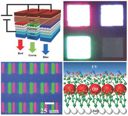
Quantum dot (QD) light‐emitting diodes have been intensively investigated as a future display technology owing to their outstanding optoelectronic properties such as narrow spectral bandwidths and high quantum efficiencies. Significant efforts have been made to achieve full color QD light‐emitting diodes (QLEDs) by applying various fine‐patterning technologies to active QD layers. However, the reported patterning methods generally require high processing cost and complex facilities which have limited their wide adoption in industrial‐scale display applications. In this study, a fine patterning method is presented by employing spatial light‐assisted and locally controlled surface tailoring. The chemical functionality of an interfacial polyethyleneimine (PEI) layer between ZnO and the QD layers is locally controlled by spatial light patterning (SLP), which is simultaneously used as a charge transfer layer and an anchoring agent for the selected QD nanoparticles. The versatility of this approach is demonstrated by patterning crossed stripes and multicolor QLED devices on selectively patterned PEI layers with a maximum luminescence of 1950 cd m−2 and a current efficiency of 2.9 cd A−1. The SLP process described herein is a general approach for fabricating full color QLEDs with marginal toxicity. This process is compatible with the standard complementary metal‐oxide semiconductor (CMOS) processing technology.
中文翻译:

全彩色量子点显示器的空间光图案化由局部控制的表面裁切实现
量子点(QD)发光二极管由于其出色的光电特性(例如窄的光谱带宽和高的量子效率)已被广泛研究作为未来的显示技术。通过将各种精细图案化技术应用于有源QD层,为实现全色QD发光二极管(QLED)做出了巨大的努力。但是,所报道的构图方法通常需要较高的处理成本和复杂的设备,这限制了它们在工业规模的显示应用中的广泛采用。在这项研究中,通过使用空间光辅助和局部控制的表面剪裁提出了一种精细的构图方法。ZnO和QD层之间的界面聚乙烯亚胺(PEI)层的化学功能由空间光图案(SLP)局部控制,它同时用作所选QD纳米粒子的电荷转移层和锚固剂。这种方法的多功能性通过在选择性图案化的PEI层上图案化交叉条纹和多色QLED器件来证明,其最大发光度为1950 cd m-2和2.9 cd A -1的电流效率。本文所述的SLP工艺是用于制造具有边际毒性的全色QLED的通用方法。此过程与标准互补金属氧化物半导体(CMOS)处理技术兼容。
更新日期:2018-03-07
中文翻译:
全彩色量子点显示器的空间光图案化由局部控制的表面裁切实现
量子点(QD)发光二极管由于其出色的光电特性(例如窄的光谱带宽和高的量子效率)已被广泛研究作为未来的显示技术。通过将各种精细图案化技术应用于有源QD层,为实现全色QD发光二极管(QLED)做出了巨大的努力。但是,所报道的构图方法通常需要较高的处理成本和复杂的设备,这限制了它们在工业规模的显示应用中的广泛采用。在这项研究中,通过使用空间光辅助和局部控制的表面剪裁提出了一种精细的构图方法。ZnO和QD层之间的界面聚乙烯亚胺(PEI)层的化学功能由空间光图案(SLP)局部控制,它同时用作所选QD纳米粒子的电荷转移层和锚固剂。这种方法的多功能性通过在选择性图案化的PEI层上图案化交叉条纹和多色QLED器件来证明,其最大发光度为1950 cd m-2和2.9 cd A -1的电流效率。本文所述的SLP工艺是用于制造具有边际毒性的全色QLED的通用方法。此过程与标准互补金属氧化物半导体(CMOS)处理技术兼容。


 京公网安备 11010802027423号