当前位置:
X-MOL 学术
›
Adv. Mater.
›
论文详情
Our official English website, www.x-mol.net, welcomes your
feedback! (Note: you will need to create a separate account there.)
A Voltage‐Boosting Strategy Enabling a Low‐Frequency, Flexible Electromagnetic Wave Absorption Device
Advanced Materials ( IF 27.4 ) Pub Date : 2018-03-07 , DOI: 10.1002/adma.201706343 Hualiang Lv 1, 2 , Zhihong Yang 1 , Paul Luyuan Wang 2 , Guangbin Ji 1 , Jizhong Song 3 , Lirong Zheng 4 , Haibo Zeng 3 , Zhichuan J. Xu 2
Advanced Materials ( IF 27.4 ) Pub Date : 2018-03-07 , DOI: 10.1002/adma.201706343 Hualiang Lv 1, 2 , Zhihong Yang 1 , Paul Luyuan Wang 2 , Guangbin Ji 1 , Jizhong Song 3 , Lirong Zheng 4 , Haibo Zeng 3 , Zhichuan J. Xu 2
Affiliation
|
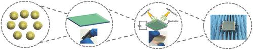
Nowadays, low‐frequency electromagnetic interference (<2.0 GHz) remains a key core issue that plagues the effective attenuation performance of conventional absorption devices prepared via the component‐morphology method (Strategy I). According to theoretical calculations, one fundamental solution is to develop a material that possesses a high ε′ but lower ε″. Thus, it is attempted to control the dielectric values via applying an external electrical field, which inducts changes in the macrostructure toward a performance improvement (Strategy II). A sandwich‐structured flexible electronic absorption device is designed using a carbon film electrode to conduct an external current. Simultaneously, an absorption layer that is highly responsive to an external voltage is selected via Strategy I. Relying on the synergistic effects from Strategies I and II, this device demonstrates an absorption value of more than 85% at 1.5–2.0 GHz with an applied voltage of 16 V while reducing the thickness to ≈5 mm. In addition, the device also shows a good absorption property at 25–150 °C. The method of utilizing an external voltage to break the intrinsic dielectric feature by modifying a traditional electronic absorption device is demonstrated for the first time and has great significance in solving the low‐frequency electromagnetic interference issue.
中文翻译:

一种电压提升策略,可实现低频,灵活的电磁波吸收装置
如今,低频电磁干扰(<2.0 GHz)仍然是困扰通过组件形态方法制备的常规吸收装置的有效衰减性能的关键核心问题(策略I)。根据理论计算,一种基本的解决方案是开发一种具有较高ε'但较低ε''的材料。因此,尝试通过施加外部电场来控制介电值,这会导致宏观结构的变化,从而提高性能(策略II)。采用碳膜电极设计的三明治结构柔性电子吸收装置可传导外部电流。同时,通过策略I选择对外部电压具有高度响应性的吸收层。依靠策略I和II的协同效应,该器件在1.5–2.0 GHz的施加电压16 V下显示出超过85%的吸收值,同时将厚度减小至≈5mm。此外,该器件在25–150°C下也显示出良好的吸收性能。首次演示了通过修改传统的电子吸收装置来利用外部电压破坏固有介电特征的方法,这对解决低频电磁干扰问题具有重要意义。
更新日期:2018-03-07
中文翻译:
一种电压提升策略,可实现低频,灵活的电磁波吸收装置
如今,低频电磁干扰(<2.0 GHz)仍然是困扰通过组件形态方法制备的常规吸收装置的有效衰减性能的关键核心问题(策略I)。根据理论计算,一种基本的解决方案是开发一种具有较高ε'但较低ε''的材料。因此,尝试通过施加外部电场来控制介电值,这会导致宏观结构的变化,从而提高性能(策略II)。采用碳膜电极设计的三明治结构柔性电子吸收装置可传导外部电流。同时,通过策略I选择对外部电压具有高度响应性的吸收层。依靠策略I和II的协同效应,该器件在1.5–2.0 GHz的施加电压16 V下显示出超过85%的吸收值,同时将厚度减小至≈5mm。此外,该器件在25–150°C下也显示出良好的吸收性能。首次演示了通过修改传统的电子吸收装置来利用外部电压破坏固有介电特征的方法,这对解决低频电磁干扰问题具有重要意义。


 京公网安备 11010802027423号