当前位置:
X-MOL 学术
›
Adv. Electron. Mater.
›
论文详情
Our official English website, www.x-mol.net, welcomes your
feedback! (Note: you will need to create a separate account there.)
Wafer Scale Transfer of Ultrathin Silicon Chips on Flexible Substrates for High Performance Bendable Systems
Advanced Electronic Materials ( IF 5.3 ) Pub Date : 2018-03-01 , DOI: 10.1002/aelm.201700277 William Taube Navaraj 1 , Shoubhik Gupta 1 , Leandro Lorenzelli 2 , Ravinder Dahiya 1
Advanced Electronic Materials ( IF 5.3 ) Pub Date : 2018-03-01 , DOI: 10.1002/aelm.201700277 William Taube Navaraj 1 , Shoubhik Gupta 1 , Leandro Lorenzelli 2 , Ravinder Dahiya 1
Affiliation
|
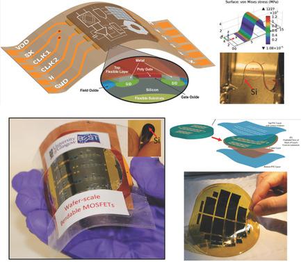
This paper presents an innovative approach for wafer scale transfer of ultrathin silicon chips on flexible substrates. The methodology is demonstrated with various devices (ultrathin chip resistive samples, metal oxide semiconductor (MOS) capacitors and n‐channel metal oxide semiconductor field effect transistors (MOSFETs)) on wafers up to 4″ diameter. This is supported by extensive electromechanical characterization and theoretical analysis, including finite element simulation, to evaluate the effect of bending and the critical breaking radius of curvature. The ultrathin chips on polyimide did not break until the radius of curvature of 1.437 mm. In the case of MOS capacitors the measured capacitance increases with increase in bending load. The changes in the transfer and output characteristics of ultrathin MOSFETs closely match with the theoretical model utilizing empirically determined parameters. Overall, the work demonstrates the efficacy of the new methodology presented here for wafer scale transfer of ultrathin chips on flexible substrates. The presented research will be useful for obtaining high performance and compact circuits needed in many futuristic flexible electronics applications such as implantable electronics and flexible displays. Further, it will open new avenues for realizing multilayered multimaterial (foil‐to‐foil) integrated bendable electronics.
中文翻译:

用于高性能可弯曲系统的柔性基板上超薄硅芯片的晶圆级转移
本文提出了一种创新方法,用于在柔性基板上超薄硅芯片的晶圆规模转移。在直径最大为4英寸的晶片上使用各种设备(超薄芯片电阻性样品,金属氧化物半导体(MOS)电容器和n沟道金属氧化物半导体场效应晶体管(MOSFET))证明了该方法。广泛的机电特性和包括有限元模拟在内的理论分析为评估弯曲的影响和临界断裂曲率半径提供了支持。直到1.437毫米的曲率半径,聚酰亚胺上的超薄切片才断裂。对于MOS电容器,测得的电容会随着弯曲负载的增加而增加。超薄MOSFET的传输和输出特性的变化与使用经验确定的参数的理论模型非常吻合。总的来说,这项工作证明了此处介绍的新方法对于在柔性基板上超薄芯片的晶圆规模转移的功效。提出的研究将对获得许多未来的柔性电子应用(如可植入电子和柔性显示器)所需的高性能和紧凑型电路很有用。此外,它将为实现多层多材料(箔对箔)集成可弯曲电子技术开辟新途径。提出的研究将对获得许多未来的柔性电子应用(如可植入电子和柔性显示器)所需的高性能和紧凑型电路很有用。此外,它将为实现多层多材料(箔对箔)集成可弯曲电子技术开辟新途径。提出的研究将对获得许多未来的柔性电子应用(如可植入电子和柔性显示器)所需的高性能和紧凑型电路很有用。此外,它将为实现多层多材料(箔对箔)集成可弯曲电子技术开辟新途径。
更新日期:2018-03-01
中文翻译:
用于高性能可弯曲系统的柔性基板上超薄硅芯片的晶圆级转移
本文提出了一种创新方法,用于在柔性基板上超薄硅芯片的晶圆规模转移。在直径最大为4英寸的晶片上使用各种设备(超薄芯片电阻性样品,金属氧化物半导体(MOS)电容器和n沟道金属氧化物半导体场效应晶体管(MOSFET))证明了该方法。广泛的机电特性和包括有限元模拟在内的理论分析为评估弯曲的影响和临界断裂曲率半径提供了支持。直到1.437毫米的曲率半径,聚酰亚胺上的超薄切片才断裂。对于MOS电容器,测得的电容会随着弯曲负载的增加而增加。超薄MOSFET的传输和输出特性的变化与使用经验确定的参数的理论模型非常吻合。总的来说,这项工作证明了此处介绍的新方法对于在柔性基板上超薄芯片的晶圆规模转移的功效。提出的研究将对获得许多未来的柔性电子应用(如可植入电子和柔性显示器)所需的高性能和紧凑型电路很有用。此外,它将为实现多层多材料(箔对箔)集成可弯曲电子技术开辟新途径。提出的研究将对获得许多未来的柔性电子应用(如可植入电子和柔性显示器)所需的高性能和紧凑型电路很有用。此外,它将为实现多层多材料(箔对箔)集成可弯曲电子技术开辟新途径。提出的研究将对获得许多未来的柔性电子应用(如可植入电子和柔性显示器)所需的高性能和紧凑型电路很有用。此外,它将为实现多层多材料(箔对箔)集成可弯曲电子技术开辟新途径。


 京公网安备 11010802027423号