当前位置:
X-MOL 学术
›
ACS Photonics
›
论文详情
Our official English website, www.x-mol.net, welcomes your
feedback! (Note: you will need to create a separate account there.)
Nano-Alignment in Semiconducting Polymer Films: A Path to Achieve High Current Density and Brightness in Organic Light Emitting Transistors
ACS Photonics ( IF 6.5 ) Pub Date : 2018-02-27 00:00:00 , DOI: 10.1021/acsphotonics.8b00011 Mujeeb Ullah Chaudhry 1 , Khalid Muhieddine 1 , Robert Wawrzinek 1 , Jun Li 2 , Shih-Chun Lo 3 , Ebinazar B. Namdas 1
ACS Photonics ( IF 6.5 ) Pub Date : 2018-02-27 00:00:00 , DOI: 10.1021/acsphotonics.8b00011 Mujeeb Ullah Chaudhry 1 , Khalid Muhieddine 1 , Robert Wawrzinek 1 , Jun Li 2 , Shih-Chun Lo 3 , Ebinazar B. Namdas 1
Affiliation
|
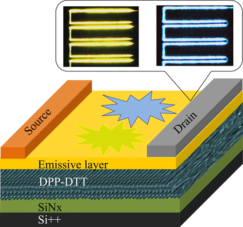
Organic light emitting field effect transistors (LEFETs) integrate light emission of a diode with logic functions of a transistor into a single device architecture. This integration has the potential to provide simplified displays at low costs and access to injection lasing. However, the charge carrier mobility in LEFETs is a limiting factor in realizing high current densities along with a trade-off between brightness and efficiency. Herein, we present a technique controlling the nanoscale morphology of semiconducting polymers using nanoscale grooved substrates and dip-coating deposition to achieve high current density. We then applied this approach to heterostructure LEFETs and demonstrated brightness exceeding 29000 cd m–2 at an EQE of 0.4% for a yellow emitter and 9600 cd m–2 at an EQE of 0.7% for a blue emitter. These results represent a significant advancement in organic optoelectronics and are an important milestone toward the realization of new applications in displays and electrically pumped lasing.
中文翻译:

半导体聚合物薄膜中的纳米排列:在有机发光晶体管中实现高电流密度和亮度的途径
有机发光场效应晶体管(LEFET)将具有晶体管逻辑功能的二极管发光集成到单个器件架构中。这种集成有潜力以低成本提供简化的显示,并具有注入激光的能力。然而,LEFET中的电荷载流子迁移率是实现高电流密度以及亮度和效率之间的权衡的限制因素。在本文中,我们提出了一种技术,该技术使用纳米级带沟槽的基板和浸涂沉积来控制半导体聚合物的纳米级形态,以实现高电流密度。然后,我们将这种方法应用于异质结构LEFET,并证明了黄色发射极和9600 cd m –2的亮度超过29000 cd m –2的EQE为0.4%。蓝色发射器的EQE为0.7%。这些结果代表了有机光电技术的重大进步,并且是实现显示器和电泵激激光新应用的重要里程碑。
更新日期:2018-02-27
中文翻译:
半导体聚合物薄膜中的纳米排列:在有机发光晶体管中实现高电流密度和亮度的途径
有机发光场效应晶体管(LEFET)将具有晶体管逻辑功能的二极管发光集成到单个器件架构中。这种集成有潜力以低成本提供简化的显示,并具有注入激光的能力。然而,LEFET中的电荷载流子迁移率是实现高电流密度以及亮度和效率之间的权衡的限制因素。在本文中,我们提出了一种技术,该技术使用纳米级带沟槽的基板和浸涂沉积来控制半导体聚合物的纳米级形态,以实现高电流密度。然后,我们将这种方法应用于异质结构LEFET,并证明了黄色发射极和9600 cd m –2的亮度超过29000 cd m –2的EQE为0.4%。蓝色发射器的EQE为0.7%。这些结果代表了有机光电技术的重大进步,并且是实现显示器和电泵激激光新应用的重要里程碑。


 京公网安备 11010802027423号