Journal of the Taiwan Institute of Chemical Engineers ( IF 5.5 ) Pub Date : 2018-02-27 , DOI: 10.1016/j.jtice.2018.01.051 Ravi Kant Tripathi , O.S. Panwar , Ishpal Rawal , B.P. Singh , B.C. Yadav
|
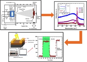
This paper reports the synthesis and properties of as grown and hydrogenated nanocrystalline silicon (nc-Si or nc-Si:H) thin films deposited by the filtered cathodic vacuum arc technique using boron doped solid silicon as a cathode. No hazardous gases like silane, diborane etc. (which are used in the conventional growth techniques) were used for the growth of nc-Si or nc-Si:H films in this process. These films have been characterized by X-ray diffraction (XRD), scanning electron microscopy, UV–visible spectroscopy, Fourier transform infrared spectroscopy, Raman spectroscopy and photo detection measurements. The XRD patterns show the amorphous and nanocrystalline coexisting nature of the films deposited under different deposition conditions. Raman spectra also reveal the amorphous nature of the film deposited at room temperature, whereas the films deposited at high temperature and under hydrogen environment silicon films showed the nanocrystalline nature. The evaluated values of dark conductivity (σD), activation energy (ΔE), optical band gap (Eg) vary from 3.6 × 10⁻⁵ to 7.2 × 10⁻³ ohm−1 cm−1, from 0.55 to 0.24 eV and from 1.24 to 2.12 eV, respectively, in nc-Si or nc-Si:H films. The fast response and recovery time as 4.92 and 4.06 s have been observed for the photo detectors developed from the nc-Si:H films deposited at room temperature.
中文翻译:
硼掺杂固体硅的阴极过滤阴极电弧弧技术生长的纳米硅薄膜用于快速光检测器的研究。
本文报道了使用硼掺杂固体硅作为阴极通过过滤阴极真空电弧技术沉积和生长的氢化纳米晶硅(nc-Si或nc-Si:H)薄膜的合成和性能。在此过程中,没有使用诸如硅烷,乙硼烷等有害气体(在常规生长技术中使用)来生长nc-Si或nc-Si:H膜。这些膜的特征在于X射线衍射(XRD),扫描电子显微镜,紫外可见光谱,傅立叶变换红外光谱,拉曼光谱和光检测测量。XRD图谱显示了在不同沉积条件下沉积的膜的非晶态和纳米晶共存的性质。拉曼光谱还揭示了在室温下沉积的薄膜的无定形性质,而在高温和氢环境下沉积的膜则显示出纳米晶的性质。暗电导率的评估值(σ d),活化能(Δ ë),光带隙(Ë克)变化从3.6×10 -5至7.2×10 -3 欧姆-1 厘米-1,0.55〜0.24 eV和从1.24到2.12电子伏特,分别在nc-Si或nc-Si:H膜中。对于在室温下沉积的nc-Si:H薄膜开发的光电探测器,已观察到4.92和4.06 s的快速响应和恢复时间。


 京公网安备 11010802027423号