当前位置:
X-MOL 学术
›
Adv. Electron. Mater.
›
论文详情
Our official English website, www.x-mol.net, welcomes your
feedback! (Note: you will need to create a separate account there.)
Bulk‐Like Electrical Properties Induced by Contact‐Limited Charge Transport in Organic Diodes: Revised Space Charge Limited Current
Advanced Electronic Materials ( IF 5.3 ) Pub Date : 2018-02-22 , DOI: 10.1002/aelm.201700493 Guangwei Xu 1, 2 , Nan Gao 1, 2 , Congyan Lu 1, 2 , Wei Wang 1, 2 , Zhuoyu Ji 1, 2 , Chong Bi 1, 2 , Zhiheng Han 1, 2 , Nianduan Lu 1, 2 , Guanhua Yang 1, 2 , Yuan Li 3 , Qi Liu 1, 2 , Ling Li 1, 2 , Ming Liu 1, 2
Advanced Electronic Materials ( IF 5.3 ) Pub Date : 2018-02-22 , DOI: 10.1002/aelm.201700493 Guangwei Xu 1, 2 , Nan Gao 1, 2 , Congyan Lu 1, 2 , Wei Wang 1, 2 , Zhuoyu Ji 1, 2 , Chong Bi 1, 2 , Zhiheng Han 1, 2 , Nianduan Lu 1, 2 , Guanhua Yang 1, 2 , Yuan Li 3 , Qi Liu 1, 2 , Ling Li 1, 2 , Ming Liu 1, 2
Affiliation
|
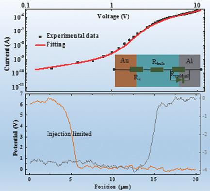
Charge transport governs the operation and performance of organic diodes. Illuminating the charge‐transfer/transport processes across the interfaces and the bulk organic semiconductors is at the focus of intensive investigations. Traditionally, the charge transport properties of organic diodes are usually characterized by probing the current–voltage (I–V) curves of the devices. However, to unveil the landscape of the underlying potential/charge distribution, which essentially determines the I–V characteristics, still represents a major challenge. Here, the electrical potential distribution in planar organic diodes is investigated by using the scanning Kelvin probe force microscopy technique, a method that can clearly separate the contact and bulk regimes of charge transport. Interestingly, by applying to devices based on novel, high mobility organic materials, the space‐charge‐limited‐current‐like I–V curves, which are previously believed to be a result of the bulk transport, are surprisingly but unambiguously demonstrated to be caused by contact‐limited conduction. A model accounting is developed for the transport properties of both the two metal/organic interfaces and the bulk. The results indicate that pure interface‐dominated transport can indeed give rise to I–V curves similar to those caused by bulk transport. These findings provide a new insight into the charge injection and transport processes in organic diodes.
中文翻译:

接触限制的有机二极管中的电荷传输引起的类似体电性质:修正的空间电荷限制电流
电荷传输控制有机二极管的操作和性能。深入研究的重点是阐明跨界面和大块有机半导体的电荷转移/传输过程。传统上,有机二极管的电荷传输性能,通常其特征在于,探测所述电流-电压(我- V)的装置的曲线。然而,揭开潜在的电势/电荷分布的面貌,从根本上决定了I – V特色,仍然代表着重大挑战。在这里,通过使用扫描开尔文探针力显微镜技术研究平面有机二极管中的电势分布,该技术可以清楚地区分电荷传输的接触和体态。有趣的是,通过应用到基于新型高迁移率有机材料的设备上,令人惊讶但明确地证明了以前被认为是大量运输的结果的像空间电荷受限电流一样的I – V曲线。由接触受限的传导引起的。针对两种金属/有机界面和块体的传输特性,开发了一种模型计算方法。结果表明,纯接口为主的传输确实可以引起I – V曲线类似于散装运输引起的曲线。这些发现为有机二极管中的电荷注入和传输过程提供了新的见解。
更新日期:2018-02-22
中文翻译:
接触限制的有机二极管中的电荷传输引起的类似体电性质:修正的空间电荷限制电流
电荷传输控制有机二极管的操作和性能。深入研究的重点是阐明跨界面和大块有机半导体的电荷转移/传输过程。传统上,有机二极管的电荷传输性能,通常其特征在于,探测所述电流-电压(我- V)的装置的曲线。然而,揭开潜在的电势/电荷分布的面貌,从根本上决定了I – V特色,仍然代表着重大挑战。在这里,通过使用扫描开尔文探针力显微镜技术研究平面有机二极管中的电势分布,该技术可以清楚地区分电荷传输的接触和体态。有趣的是,通过应用到基于新型高迁移率有机材料的设备上,令人惊讶但明确地证明了以前被认为是大量运输的结果的像空间电荷受限电流一样的I – V曲线。由接触受限的传导引起的。针对两种金属/有机界面和块体的传输特性,开发了一种模型计算方法。结果表明,纯接口为主的传输确实可以引起I – V曲线类似于散装运输引起的曲线。这些发现为有机二极管中的电荷注入和传输过程提供了新的见解。


 京公网安备 11010802027423号