当前位置:
X-MOL 学术
›
Adv. Electron. Mater.
›
论文详情
Our official English website, www.x-mol.net, welcomes your
feedback! (Note: you will need to create a separate account there.)
Interface Modulation and Optimization of Electrical Properties of HfGdO/GaAs Gate Stacks by ALD‐Derived Al2O3 Passivation Layer and Forming Gas Annealing
Advanced Electronic Materials ( IF 5.3 ) Pub Date : 2018-02-19 , DOI: 10.1002/aelm.201700543 Shanshan Jiang 1 , Gang He 1 , Mao Liu 2 , Li Zhu 1 , Shuang Liang 1 , Wendong Li 1 , Zhaoqi Sun 1 , Mingliang Tian 1, 3
Advanced Electronic Materials ( IF 5.3 ) Pub Date : 2018-02-19 , DOI: 10.1002/aelm.201700543 Shanshan Jiang 1 , Gang He 1 , Mao Liu 2 , Li Zhu 1 , Shuang Liang 1 , Wendong Li 1 , Zhaoqi Sun 1 , Mingliang Tian 1, 3
Affiliation
|
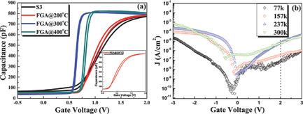
Metal‐oxide‐semiconductor (MOS) capacitors with sputtering‐deposited Gd‐doped HfO2(HGO) high k gate dielectric thin films and ALD‐derived Al2O3 interfacial passivation layer were fabricated on GaAs substrates. The effects of the passivation layer and the forming gas annealing (FGA) temperature were explored by studying the interfacial chemical bonding states and electrical properties of HGO/GaAs and HGO/Al2O3/GaAs gate stacks via x‐ray photoelectron spectroscopy (XPS), capacitance‐voltage (C–V), and leakage current density‐voltage ( J–V) measurements. Results indicated that the MOS capacitors performances were enhanced by performing FGA. The electrical analysis revealed that the 300 °C‐annealed Al/HGO/GaAs/Al MOS capacitor with 20 cycles Al2O3 passivation layer experienced improved electrical properties, with a dielectric constant of 44, a flat band voltage of 0.64 V, a hysteresis of 0.02 V corresponding to the oxide charge density of −6.2 × 1012 cm2, border trapped oxide charge density of −3.02 × 1011 cm2, a leakage current density 5.87 × 10‐6 A/cm2 at a bias voltage of 2 V. The low temperature (77–300 K) dependent detailed current conduction mechanisms (CCMs) of the 300 °C‐annealed MOS capacitor at low temperatures were also systematically investigated. The optimized interface chemistry and the excellent electrical properties suggested that HGO/Al2O3/GaAs potential gate stacks could be applied in future III‐V‐based MOSFET devices.
中文翻译:

ALD衍生的Al2O3钝化层和气体退火对HfGdO / GaAs栅堆叠的界面调制和电性能的优化
在GaAs衬底上制造了具有溅射沉积的掺Gd的HfO 2(HGO)高k栅极电介质薄膜和ALD衍生的Al 2 O 3界面钝化层的金属氧化物半导体(MOS)电容器。通过X射线光电子能谱(XPS)研究了HGO / GaAs和HGO / Al 2 O 3 / GaAs栅堆叠的界面化学键合状态和电学性质,探讨了钝化层和形成气体退火(FGA)温度的影响。),电容电压(C–V)和漏电流密度电压( J–V)) 测量。结果表明,通过进行FGA可以提高MOS电容器的性能。电气分析表明,经过300°C退火的Al / HGO / GaAs / Al MOS电容器具有20个循环的Al 2 O 3钝化层,其电性能有所改善,介电常数为44,平带电压为0.64 V, 0.02 V的磁滞,对应于-6.2×10 12 cm 2的氧化物电荷密度,-3.02×10 11 cm 2的边界俘获氧化物电荷密度,泄漏电流密度5.87×10 -6 A / cm 2在2 V的偏置电压下。还系统地研究了低温(77–300 K)下与300°C退火的MOS电容器在低温下有关的详细电流传导机制(CCM)。优化的界面化学性质和出色的电性能表明,HGO / Al 2 O 3 / GaAs电位栅叠层可用于未来的基于IIIV的MOSFET器件。
更新日期:2018-02-19
中文翻译:
ALD衍生的Al2O3钝化层和气体退火对HfGdO / GaAs栅堆叠的界面调制和电性能的优化
在GaAs衬底上制造了具有溅射沉积的掺Gd的HfO 2(HGO)高k栅极电介质薄膜和ALD衍生的Al 2 O 3界面钝化层的金属氧化物半导体(MOS)电容器。通过X射线光电子能谱(XPS)研究了HGO / GaAs和HGO / Al 2 O 3 / GaAs栅堆叠的界面化学键合状态和电学性质,探讨了钝化层和形成气体退火(FGA)温度的影响。),电容电压(C–V)和漏电流密度电压( J–V)) 测量。结果表明,通过进行FGA可以提高MOS电容器的性能。电气分析表明,经过300°C退火的Al / HGO / GaAs / Al MOS电容器具有20个循环的Al 2 O 3钝化层,其电性能有所改善,介电常数为44,平带电压为0.64 V, 0.02 V的磁滞,对应于-6.2×10 12 cm 2的氧化物电荷密度,-3.02×10 11 cm 2的边界俘获氧化物电荷密度,泄漏电流密度5.87×10 -6 A / cm 2在2 V的偏置电压下。还系统地研究了低温(77–300 K)下与300°C退火的MOS电容器在低温下有关的详细电流传导机制(CCM)。优化的界面化学性质和出色的电性能表明,HGO / Al 2 O 3 / GaAs电位栅叠层可用于未来的基于IIIV的MOSFET器件。


 京公网安备 11010802027423号