Our official English website, www.x-mol.net, welcomes your
feedback! (Note: you will need to create a separate account there.)
Colloidal lithography-based fabrication of highly-ordered nanofluidic channels with an ultra-high surface-to-volume ratio†
Lab on a Chip ( IF 6.1 ) Pub Date : 2018-02-20 00:00:00 , DOI: 10.1039/c7lc01326d Shuli Wang 1, 2, 3, 4, 5 , Yongshun Liu 5, 6, 7, 8, 9 , Peng Ge 1, 2, 3, 4, 5 , Qiqi Kan 1, 2, 3, 4, 5 , Nianzuo Yu 1, 2, 3, 4, 5 , Jing Wang 1, 3, 4, 5, 10 , Jingjie Nan 1, 2, 3, 4, 5 , Shunsheng Ye 1, 2, 3, 4, 5 , Junhu Zhang 1, 2, 3, 4, 5 , Weiqing Xu 1, 3, 4, 5, 10 , Bai Yang 1, 2, 3, 4, 5
Lab on a Chip ( IF 6.1 ) Pub Date : 2018-02-20 00:00:00 , DOI: 10.1039/c7lc01326d Shuli Wang 1, 2, 3, 4, 5 , Yongshun Liu 5, 6, 7, 8, 9 , Peng Ge 1, 2, 3, 4, 5 , Qiqi Kan 1, 2, 3, 4, 5 , Nianzuo Yu 1, 2, 3, 4, 5 , Jing Wang 1, 3, 4, 5, 10 , Jingjie Nan 1, 2, 3, 4, 5 , Shunsheng Ye 1, 2, 3, 4, 5 , Junhu Zhang 1, 2, 3, 4, 5 , Weiqing Xu 1, 3, 4, 5, 10 , Bai Yang 1, 2, 3, 4, 5
Affiliation
|
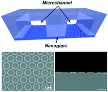
This article shows a new strategy for the fabrication of nanofluidics based on nanoscale gaps in nanopillar arrays. Silicon nanopillar arrays are prepared in a designed position by combining conventional photolithography with colloidal lithography. The nanogaps between the pillars are used as nanochannels for the connection of two polydimethylsiloxane-based microchannels in microfluidics. The gap between neighbouring nanopillars can be accurately controlled by changing the size of initial colloidal spheres and by an etching process, which further determines the dimensions of the nanochannels. At a low ionic strength, the surface charge-governed ion transportation shows that the nanochannels possess the same electrokinetic properties as typical nanofluidics. Benefiting from the advantage of photolithography, large-area nanochannel arrays can be prepared in a parallel manner. Due to the perm-selectivity of the nanochannels, the nanofluidic chips can be used to preconcentrate low concentration samples. The large-area ordered nanostructures preserve their high-throughput property and large surface-to-volume ratio, which shows their great potential in the development of nanofluidics and their applications, such as in the separation of small molecules, energy conversion, etc.
中文翻译:

基于胶体光刻技术的超有序纳米流体通道的制造,具有超高的表面体积比†
本文显示了一种基于纳米柱阵列中纳米级间隙的纳米流体制备新策略。通过将常规光刻技术与胶体光刻技术相结合,可以在设计位置制备硅纳米柱阵列。柱之间的纳米间隙用作微流体中两个聚二甲基硅氧烷基微通道连接的纳米通道。相邻纳米柱之间的间隙可以通过更改初始胶体球的大小和蚀刻工艺来精确控制,蚀刻工艺可以进一步确定纳米通道的尺寸。在低离子强度下,表面控制的离子传输表明纳米通道具有与典型的纳米流体相同的电动特性。受益于光刻的优势,可以并行方式制备大面积的纳米通道阵列。由于纳米通道的渗透选择性,纳米流体芯片可用于预浓缩低浓度样品。大面积有序纳米结构保留了其高通量特性和大的表面体积比,这表明它们在纳米流体的发展及其应用中具有巨大的潜力,例如在小分子的分离,能量转换,ETC。
更新日期:2018-02-20
中文翻译:
基于胶体光刻技术的超有序纳米流体通道的制造,具有超高的表面体积比†
本文显示了一种基于纳米柱阵列中纳米级间隙的纳米流体制备新策略。通过将常规光刻技术与胶体光刻技术相结合,可以在设计位置制备硅纳米柱阵列。柱之间的纳米间隙用作微流体中两个聚二甲基硅氧烷基微通道连接的纳米通道。相邻纳米柱之间的间隙可以通过更改初始胶体球的大小和蚀刻工艺来精确控制,蚀刻工艺可以进一步确定纳米通道的尺寸。在低离子强度下,表面控制的离子传输表明纳米通道具有与典型的纳米流体相同的电动特性。受益于光刻的优势,可以并行方式制备大面积的纳米通道阵列。由于纳米通道的渗透选择性,纳米流体芯片可用于预浓缩低浓度样品。大面积有序纳米结构保留了其高通量特性和大的表面体积比,这表明它们在纳米流体的发展及其应用中具有巨大的潜力,例如在小分子的分离,能量转换,ETC。


 京公网安备 11010802027423号