当前位置:
X-MOL 学术
›
Faraday Discuss.
›
论文详情
Our official English website, www.x-mol.net, welcomes your
feedback! (Note: you will need to create a separate account there.)
Charge transport at a molecular GaAs nanoscale junction
Faraday Discussions ( IF 3.3 ) Pub Date : 2018-02-15 , DOI: 10.1039/c8fd00016f Andrea Vezzoli 1, 2, 3, 4 , Richard J. Brooke 4, 5, 6, 7 , Nicolò Ferri 1, 2, 3, 4 , Carly Brooke 1, 2, 3, 4 , Simon J. Higgins 1, 2, 3, 4 , Walther Schwarzacher 4, 5, 6, 7 , Richard J. Nichols 1, 2, 3, 4
Faraday Discussions ( IF 3.3 ) Pub Date : 2018-02-15 , DOI: 10.1039/c8fd00016f Andrea Vezzoli 1, 2, 3, 4 , Richard J. Brooke 4, 5, 6, 7 , Nicolò Ferri 1, 2, 3, 4 , Carly Brooke 1, 2, 3, 4 , Simon J. Higgins 1, 2, 3, 4 , Walther Schwarzacher 4, 5, 6, 7 , Richard J. Nichols 1, 2, 3, 4
Affiliation
|
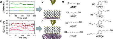
In recent years, the use of non-metallic electrodes for the fabrication of single-molecule junctions has developed into an elegant way to impart new properties to nanodevices. Integration of molecular junctions in a semiconducting platform would also speed technological deployment, as it would take advantage of established industrial infrastructures. In a previous proof-of-concept paper, we used simple α,ω-dithiol self-assembled monolayers on a gallium arsenide (GaAs) substrate to fabricate molecular Schottky diodes with a STM. In the devices, we were also able to detect the contribution of a single-molecule to the overall charge transport. The prepared devices can also be used as photodiodes, as GaAs is a III–V direct bandgap (1.42 eV at room temperature) semiconductor, and it efficiently absorbs visible light to generate a photocurrent. In this contribution, we demonstrate that fine control can be exerted on the electrical behaviour of a metal-molecule–GaAs junction by systematically altering the nature of the molecular bridge, the type and doping density of the semiconductor and the light intensity and wavelength. Molecular orbital energy alignment dominates the charge transport properties, resulting in strongly rectifying junctions prepared with saturated bridges (e.g. alkanedithiols), with increasingly ohmic characteristics as the degree of saturation is reduced through the introduction of conjugated moieties. The effects we observed are local, and may be observed with electrodes of only a few tens of nanometres in size, hence paving the way to the use of semiconducting nanoelectrodes to probe molecular properties. Perspectives of these new developments for single molecule semiconductor electrochemistry are also discussed.
中文翻译:

分子GaAs纳米级结处的电荷传输
近年来,使用非金属电极制造单分子结已发展成为一种优雅的方式,可以赋予纳米器件新的性能。分子连接在半导体平台中的集成也将加快技术的部署,因为它将利用已建立的工业基础设施。在先前的概念验证论文中,我们在砷化镓(GaAs)衬底上使用了简单的α,ω-二硫醇自组装单分子层,以制造具有STM的分子肖特基二极管。在设备中,我们还能够检测到单分子对整个电荷传输的贡献。准备好的器件也可以用作光电二极管,因为GaAs是III–V直接带隙(室温下为1.42 eV)的半导体,它可以有效吸收可见光以产生光电流。在这一贡献中,我们证明可以通过系统地改变分子桥的性质,半导体的类型和掺杂密度以及光强度和波长,对金属分子-GaAs结的电行为进行精细控制。分子轨道能量的排列控制着电荷的传输特性,从而导致用饱和电桥制备的强整流结((例如链烷二硫醇),由于引入共轭部分降低了饱和度,因此具有越来越多的欧姆特性。我们观察到的影响是局部的,并且可能仅在几十纳米大小的电极上观察到,因此为使用半导体纳米电极探测分子性质铺平了道路。还讨论了单分子半导体电化学新发展的观点。
更新日期:2018-10-10
中文翻译:
分子GaAs纳米级结处的电荷传输
近年来,使用非金属电极制造单分子结已发展成为一种优雅的方式,可以赋予纳米器件新的性能。分子连接在半导体平台中的集成也将加快技术的部署,因为它将利用已建立的工业基础设施。在先前的概念验证论文中,我们在砷化镓(GaAs)衬底上使用了简单的α,ω-二硫醇自组装单分子层,以制造具有STM的分子肖特基二极管。在设备中,我们还能够检测到单分子对整个电荷传输的贡献。准备好的器件也可以用作光电二极管,因为GaAs是III–V直接带隙(室温下为1.42 eV)的半导体,它可以有效吸收可见光以产生光电流。在这一贡献中,我们证明可以通过系统地改变分子桥的性质,半导体的类型和掺杂密度以及光强度和波长,对金属分子-GaAs结的电行为进行精细控制。分子轨道能量的排列控制着电荷的传输特性,从而导致用饱和电桥制备的强整流结((例如链烷二硫醇),由于引入共轭部分降低了饱和度,因此具有越来越多的欧姆特性。我们观察到的影响是局部的,并且可能仅在几十纳米大小的电极上观察到,因此为使用半导体纳米电极探测分子性质铺平了道路。还讨论了单分子半导体电化学新发展的观点。


 京公网安备 11010802027423号