当前位置:
X-MOL 学术
›
Adv. Funct. Mater.
›
论文详情
Our official English website, www.x-mol.net, welcomes your
feedback! (Note: you will need to create a separate account there.)
2D Nanomaterial Arrays for Electronics and Optoelectronics
Advanced Functional Materials ( IF 18.5 ) Pub Date : 2018-02-14 , DOI: 10.1002/adfm.201706559 Chuanhui Gong 1 , Kai Hu 1 , Xuepeng Wang 1 , Peihua Wangyang 1 , Chaoyi Yan 1 , Junwei Chu 1 , Min Liao 2 , Liping Dai 1 , Tianyou Zhai 3 , Chao Wang 1 , Liang Li 4 , Jie Xiong 1
Advanced Functional Materials ( IF 18.5 ) Pub Date : 2018-02-14 , DOI: 10.1002/adfm.201706559 Chuanhui Gong 1 , Kai Hu 1 , Xuepeng Wang 1 , Peihua Wangyang 1 , Chaoyi Yan 1 , Junwei Chu 1 , Min Liao 2 , Liping Dai 1 , Tianyou Zhai 3 , Chao Wang 1 , Liang Li 4 , Jie Xiong 1
Affiliation
|
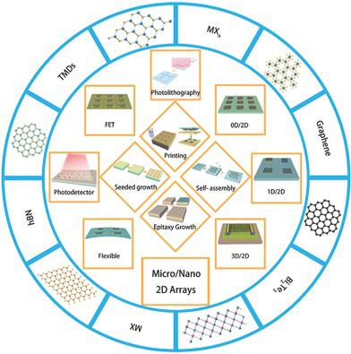
Two‐dimensional (2D) materials, benefitting from their unique planar structure and various appealing electronic properties, have attracted much attention for novel electronic and optoelectronic applications. As a basis for practical devices, the study of micro/nano‐2D material arrays based on coupling effects and synergistic effects is critical to the functionalization and integration of 2D materials. Moreover, micro/nano‐2D material arrays are compatible with traditional complementary metal oxide semiconductor (CMOS) electronics, catering well to high‐integration, high‐sensitivity, and low‐cost sensing and imaging systems. This review presents some recent studies on 2D material arrays in sequence from their novel preparations to high‐integration applications as well as explorations on dimension tuning. A first focus is on various typical fabrication methods for 2D material arrays, including photolithography, 2D printing, seeded growth, van der Waals epitaxial growth, and self‐assembly. Then, the applications of 2D material arrays, such as field effect transistors, photodetectors, pressure sensors, as well as flexible electronic devices of photodetectors and strain sensors, are elaborately introduced. Furthermore, the recent burgeoning exploration of mixed‐dimensional heterostructure arrays including 0D/2D, 1D/2D, and 3D/2D is discussed. Ultimately, conclusions and an outlook based on the current developments in this promising field are presented.
中文翻译:

电子和光电的2D纳米材料阵列
二维(2D)材料得益于其独特的平面结构和各种吸引人的电子特性,已在新型电子和光电应用领域引起了广泛关注。作为实际设备的基础,基于耦合效应和协同效应的微米/纳米2D材料阵列的研究对于2D材料的功能化和集成至关重要。此外,微米/纳米2D材料阵列与传统的互补金属氧化物半导体(CMOS)电子产品兼容,非常适合于高集成度,高灵敏度以及低成本的传感和成像系统。这篇综述按顺序提出了一些有关二维材料阵列的最新研究,从其新颖的制备到高集成度的应用,以及对尺寸调整的探索。第一个重点是用于2D材料阵列的各种典型制造方法,包括光刻,2D打印,种子生长,范德华外延生长和自组装。然后,详细介绍了二维材料阵列的应用,例如场效应晶体管,光电探测器,压力传感器以及光电探测器和应变传感器的柔性电子设备。此外,讨论了包括0D / 2D,1D / 2D和3D / 2D在内的混合维异质结构阵列的新兴探索。最终,提出了基于该有前途领域的当前发展的结论和展望。诸如场效应晶体管,光电探测器,压力传感器以及光电探测器和应变传感器的柔性电子设备等详细介绍。此外,讨论了包括0D / 2D,1D / 2D和3D / 2D在内的混合维异质结构阵列的新兴探索。最终,提出了基于该有前途领域的当前发展的结论和展望。诸如场效应晶体管,光电探测器,压力传感器以及光电探测器和应变传感器的柔性电子设备等详细介绍。此外,讨论了包括0D / 2D,1D / 2D和3D / 2D在内的混合维异质结构阵列的新兴探索。最终,提出了基于该有前途领域的当前发展的结论和展望。
更新日期:2018-02-14
中文翻译:
电子和光电的2D纳米材料阵列
二维(2D)材料得益于其独特的平面结构和各种吸引人的电子特性,已在新型电子和光电应用领域引起了广泛关注。作为实际设备的基础,基于耦合效应和协同效应的微米/纳米2D材料阵列的研究对于2D材料的功能化和集成至关重要。此外,微米/纳米2D材料阵列与传统的互补金属氧化物半导体(CMOS)电子产品兼容,非常适合于高集成度,高灵敏度以及低成本的传感和成像系统。这篇综述按顺序提出了一些有关二维材料阵列的最新研究,从其新颖的制备到高集成度的应用,以及对尺寸调整的探索。第一个重点是用于2D材料阵列的各种典型制造方法,包括光刻,2D打印,种子生长,范德华外延生长和自组装。然后,详细介绍了二维材料阵列的应用,例如场效应晶体管,光电探测器,压力传感器以及光电探测器和应变传感器的柔性电子设备。此外,讨论了包括0D / 2D,1D / 2D和3D / 2D在内的混合维异质结构阵列的新兴探索。最终,提出了基于该有前途领域的当前发展的结论和展望。诸如场效应晶体管,光电探测器,压力传感器以及光电探测器和应变传感器的柔性电子设备等详细介绍。此外,讨论了包括0D / 2D,1D / 2D和3D / 2D在内的混合维异质结构阵列的新兴探索。最终,提出了基于该有前途领域的当前发展的结论和展望。诸如场效应晶体管,光电探测器,压力传感器以及光电探测器和应变传感器的柔性电子设备等详细介绍。此外,讨论了包括0D / 2D,1D / 2D和3D / 2D在内的混合维异质结构阵列的新兴探索。最终,提出了基于该有前途领域的当前发展的结论和展望。


 京公网安备 11010802027423号