Our official English website, www.x-mol.net, welcomes your
feedback! (Note: you will need to create a separate account there.)
Single crystal diamond membranes for nanoelectronics†
Nanoscale ( IF 5.8 ) Pub Date : 2018-01-30 00:00:00 , DOI: 10.1039/c7nr09097h Kerem Bray 1, 2, 3, 4 , Hiromitsu Kato 5, 6, 7, 8 , Rodolfo Previdi 1, 2, 3, 4 , Russell Sandstrom 1, 2, 3, 4 , Kumaravelu Ganesan 4, 9, 10, 11 , Masahiko Ogura 5, 6, 7, 8 , Toshiharu Makino 5, 6, 7, 8 , Satoshi Yamasaki 5, 6, 7, 8 , Andrew P. Magyar 12, 13, 14 , Milos Toth 1, 2, 3, 4 , Igor Aharonovich 1, 2, 3, 4
Nanoscale ( IF 5.8 ) Pub Date : 2018-01-30 00:00:00 , DOI: 10.1039/c7nr09097h Kerem Bray 1, 2, 3, 4 , Hiromitsu Kato 5, 6, 7, 8 , Rodolfo Previdi 1, 2, 3, 4 , Russell Sandstrom 1, 2, 3, 4 , Kumaravelu Ganesan 4, 9, 10, 11 , Masahiko Ogura 5, 6, 7, 8 , Toshiharu Makino 5, 6, 7, 8 , Satoshi Yamasaki 5, 6, 7, 8 , Andrew P. Magyar 12, 13, 14 , Milos Toth 1, 2, 3, 4 , Igor Aharonovich 1, 2, 3, 4
Affiliation
|
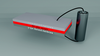
Single crystal, nanoscale diamond membranes are highly sought after for a variety of applications including nanophotonics, nanoelectronics and quantum information science. However, so far, the availability of conductive diamond membranes has remained an unreachable goal. In this work we present a complete nanofabrication methodology for engineering high aspect ratio, electrically active single crystal diamond membranes. The membranes have large lateral directions, exceeding ∼500 × 500 μm2 and are only several hundreds of nanometers thick. We further realize vertical single crystal p–n junctions made from the diamond membranes that exhibit onset voltages of ∼10 V and a current of several mA. Moreover, we deterministically introduce optically active color centers into the membranes, and demonstrate for the first time a single crystal nanoscale diamond LED. The robust and scalable approach to engineer the electrically active single crystal diamond membranes offers new pathways for advanced nanophotonic, nanoelectronic and optomechanical devices employing diamond.
中文翻译:

用于纳米电子学的单晶金刚石膜†
单晶纳米级金刚石膜在包括纳米光子学,纳米电子学和量子信息科学在内的各种应用中都倍受追捧。然而,到目前为止,导电金刚石膜的可用性仍然是无法实现的目标。在这项工作中,我们提出了一种完整的纳米加工方法,可用于工程化高深宽比,电活性单晶金刚石膜。膜具有大的横向方向,超过约500×500微米2并且只有几百纳米厚。我们进一步实现了由金刚石膜制成的垂直单晶p–n结,这些结表现出约10 V的起始电压和几mA的电流。此外,我们确定性地将光学活性色心引入膜中,并首次展示了单晶纳米级金刚石LED。设计电活性单晶金刚石膜的强大且可扩展的方法为采用金刚石的先进纳米光子,纳米电子和光机械设备提供了新途径。
更新日期:2018-01-30
中文翻译:
用于纳米电子学的单晶金刚石膜†
单晶纳米级金刚石膜在包括纳米光子学,纳米电子学和量子信息科学在内的各种应用中都倍受追捧。然而,到目前为止,导电金刚石膜的可用性仍然是无法实现的目标。在这项工作中,我们提出了一种完整的纳米加工方法,可用于工程化高深宽比,电活性单晶金刚石膜。膜具有大的横向方向,超过约500×500微米2并且只有几百纳米厚。我们进一步实现了由金刚石膜制成的垂直单晶p–n结,这些结表现出约10 V的起始电压和几mA的电流。此外,我们确定性地将光学活性色心引入膜中,并首次展示了单晶纳米级金刚石LED。设计电活性单晶金刚石膜的强大且可扩展的方法为采用金刚石的先进纳米光子,纳米电子和光机械设备提供了新途径。


 京公网安备 11010802027423号