当前位置:
X-MOL 学术
›
J. Anal. At. Spectrom.
›
论文详情
Our official English website, www.x-mol.net, welcomes your
feedback! (Note: you will need to create a separate account there.)
Technical note: Characterization of gold coated ceramics by radiofrequency pulsed glow discharge – time of flight mass spectrometry
Journal of Analytical Atomic Spectrometry ( IF 3.1 ) Pub Date : 2018-01-30 00:00:00 , DOI: 10.1039/c7ja00419b Marcos Bouza 1, 2, 3, 4, 5 , Lara Lobo 1, 2, 3, 4, 5 , Rocío Muñiz 1, 2, 3, 4, 5 , Rosario Pereiro 1, 2, 3, 4, 5 , Joseba Esparza 5, 6, 7 , José Antonio García 5, 8, 9
Journal of Analytical Atomic Spectrometry ( IF 3.1 ) Pub Date : 2018-01-30 00:00:00 , DOI: 10.1039/c7ja00419b Marcos Bouza 1, 2, 3, 4, 5 , Lara Lobo 1, 2, 3, 4, 5 , Rocío Muñiz 1, 2, 3, 4, 5 , Rosario Pereiro 1, 2, 3, 4, 5 , Joseba Esparza 5, 6, 7 , José Antonio García 5, 8, 9
Affiliation
|
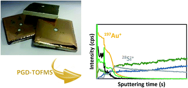
Although it is well known that glow discharge (GD) spectrometry can be used for characterization of both conductive and non-conductive materials, its application to insulators is limited and can be challenging when aiming at the analysis of thick samples. Voltage drop across the material can lead to low power deposition and so to non-efficient sputtering. In this article successful depth profile characterization studies on 6 mm thick ceramic samples coated with a thin (in the nm range) gold layer by means of a commercially available radiofrequency pulsed GD (RF-PGD) coupled time of flight mass spectrometry (RF-PGD-TOFMS) instrument are presented. Careful optimization of the operating conditions was required to achieve proper sputtering of the insulator substrate. 30 W applied rf power, 95 Pa pressure in the GD chamber and a pulse width of 500 μs with a period of 1.49 ms were selected. Characterization of a set of industrially prepared ceramic samples under different conditions was carried out. To overcome problems related to the roughness of the samples, estimation of sample thickness was achieved with an alternative approach based on the use of flat glasses with known Au layer thicknesses. Results of the investigated ceramic samples have shown Au layer thicknesses ranging between 20 and 120 nm. Moreover, screening of other metallic elements within the Au thin coating was carried out, and the presence of Rh, Bi, Pt, Ir and Pd in the Au layer was observed.
中文翻译:

技术说明:通过射频脉冲辉光放电表征镀金陶瓷–飞行时间质谱
尽管众所周知,辉光放电(GD)光谱可用于表征导电材料和非导电材料,但其在绝缘体中的应用受到限制,并且在针对厚样品的分析时可能具有挑战性。材料上的电压降会导致低功率沉积,从而导致无效溅射。在本文中,通过市售的射频脉冲GD(RF-PGD)耦合飞行时间质谱(RF-PGD),成功地对6 mm厚的薄金层(nm范围)涂层的陶瓷样品进行了深度轮廓表征研究-TOFMS)仪器。需要仔细优化操作条件以实现绝缘体基板的正确溅射。施加30 W射频功率,选择GD室中的压力为95 Pa,脉冲宽度为500μs,周期为1.49 ms。在不同条件下对一组工业制备的陶瓷样品进行了表征。为了克服与样品粗糙度相关的问题,使用基于已知Au层厚度的平板玻璃的另一种方法,可以估算出样品的厚度。所研究的陶瓷样品的结果表明,Au层的厚度在20到120 nm之间。此外,对Au薄涂层内的其他金属元素进行了筛选,并且观察到Au层中存在Rh,Bi,Pt,Ir和Pd。为了克服与样品粗糙度相关的问题,使用基于已知Au层厚度的平板玻璃的另一种方法,可以估算出样品的厚度。所研究的陶瓷样品的结果表明,Au层的厚度在20到120 nm之间。此外,对Au薄涂层内的其他金属元素进行了筛选,并且观察到Au层中存在Rh,Bi,Pt,Ir和Pd。为了克服与样品粗糙度相关的问题,使用基于已知Au层厚度的平板玻璃的另一种方法,可以估算出样品的厚度。所研究的陶瓷样品的结果表明,Au层的厚度在20到120 nm之间。此外,对Au薄涂层内的其他金属元素进行了筛选,并且观察到Au层中存在Rh,Bi,Pt,Ir和Pd。
更新日期:2018-01-30
中文翻译:
技术说明:通过射频脉冲辉光放电表征镀金陶瓷–飞行时间质谱
尽管众所周知,辉光放电(GD)光谱可用于表征导电材料和非导电材料,但其在绝缘体中的应用受到限制,并且在针对厚样品的分析时可能具有挑战性。材料上的电压降会导致低功率沉积,从而导致无效溅射。在本文中,通过市售的射频脉冲GD(RF-PGD)耦合飞行时间质谱(RF-PGD),成功地对6 mm厚的薄金层(nm范围)涂层的陶瓷样品进行了深度轮廓表征研究-TOFMS)仪器。需要仔细优化操作条件以实现绝缘体基板的正确溅射。施加30 W射频功率,选择GD室中的压力为95 Pa,脉冲宽度为500μs,周期为1.49 ms。在不同条件下对一组工业制备的陶瓷样品进行了表征。为了克服与样品粗糙度相关的问题,使用基于已知Au层厚度的平板玻璃的另一种方法,可以估算出样品的厚度。所研究的陶瓷样品的结果表明,Au层的厚度在20到120 nm之间。此外,对Au薄涂层内的其他金属元素进行了筛选,并且观察到Au层中存在Rh,Bi,Pt,Ir和Pd。为了克服与样品粗糙度相关的问题,使用基于已知Au层厚度的平板玻璃的另一种方法,可以估算出样品的厚度。所研究的陶瓷样品的结果表明,Au层的厚度在20到120 nm之间。此外,对Au薄涂层内的其他金属元素进行了筛选,并且观察到Au层中存在Rh,Bi,Pt,Ir和Pd。为了克服与样品粗糙度相关的问题,使用基于已知Au层厚度的平板玻璃的另一种方法,可以估算出样品的厚度。所研究的陶瓷样品的结果表明,Au层的厚度在20到120 nm之间。此外,对Au薄涂层内的其他金属元素进行了筛选,并且观察到Au层中存在Rh,Bi,Pt,Ir和Pd。


 京公网安备 11010802027423号