当前位置:
X-MOL 学术
›
CrystEngComm
›
论文详情
Our official English website, www.x-mol.net, welcomes your
feedback! (Note: you will need to create a separate account there.)
Kinetically controlled transition from 2D nanostructured films to 3D multifaceted InN nanocrystals on GaN(0001)
CrystEngComm ( IF 2.6 ) Pub Date : 2018-01-23 00:00:00 , DOI: 10.1039/c7ce02070h H. V. Stanchu 1, 2, 3, 4, 5 , A. V. Kuchuk 5, 6, 7, 8 , P. M. Lytvyn 1, 2, 3, 4, 9 , Yu. I. Mazur 5, 6, 7, 8 , M. E. Ware 5, 6, 7, 8 , Y. Maidaniuk 5, 6, 7, 8 , M. Benamara 5, 6, 7, 8 , Zh. M. Wang 1, 2, 3, 4 , G. J. Salamo 5, 6, 7, 8
CrystEngComm ( IF 2.6 ) Pub Date : 2018-01-23 00:00:00 , DOI: 10.1039/c7ce02070h H. V. Stanchu 1, 2, 3, 4, 5 , A. V. Kuchuk 5, 6, 7, 8 , P. M. Lytvyn 1, 2, 3, 4, 9 , Yu. I. Mazur 5, 6, 7, 8 , M. E. Ware 5, 6, 7, 8 , Y. Maidaniuk 5, 6, 7, 8 , M. Benamara 5, 6, 7, 8 , Zh. M. Wang 1, 2, 3, 4 , G. J. Salamo 5, 6, 7, 8
Affiliation
|
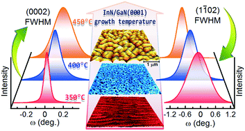
The evolution of morphological, structural, and luminescence properties of InN nanostructures grown on [0001]-oriented GaN substrates by plasma-assisted molecular beam epitaxy is reported. By varying the growth temperature, Tgr, by only 100 °C, a dramatic change in the apparent growth mechanism and the resulting surface morphology and nanoscale structure is observed. At the same time, there is a 30-fold enhancement in the photoluminescence intensity and an order of magnitude reduction in electron concentration. These changes result from a transition from a continuous 2D planar nanostructured film for the lower temperature growth characterized by high densities of edge type threading dislocations to 3D multifaceted nanocrystals with few observed dislocations for the higher temperature growth. This transition is correlated with an enhancement of the In adatom surface diffusivity due to the increased growth temperature and consequently with the dimensionality of the resulting nanostructures. Finally, it is demonstrated that understanding and implementation of the kinetic factors that influence the nucleation, growth, and crystal facet evolution during the initial stages of growth are crucial for the growth of 3D InN nanostructures or continuous layers with controllable properties.
中文翻译:

从2D纳米结构薄膜到GaN上的3D多面InN纳米晶体的动力学控制跃迁(0001)
报道了通过等离子体辅助分子束外延在[0001]取向的GaN衬底上生长的InN纳米结构的形态,结构和发光性质的演变。通过改变生长温度,T gr,仅在100°C时,观察到表观生长机理以及所产生的表面形态和纳米级结构发生了显着变化。同时,光致发光强度提高了30倍,电子浓度降低了一个数量级。这些变化是由于从以较低温度生长为特征的高密度边缘型螺纹位错的连续2D平面纳米结构薄膜过渡到3D多面纳米晶体而对于较高温度生长几乎没有观察到的位错的过渡所引起的。该转变与由于升高的生长温度而导致的In吸附原子表面扩散性的提高相关,并且因此与所得纳米结构的尺寸相关。最后,
更新日期:2018-01-23
中文翻译:
从2D纳米结构薄膜到GaN上的3D多面InN纳米晶体的动力学控制跃迁(0001)
报道了通过等离子体辅助分子束外延在[0001]取向的GaN衬底上生长的InN纳米结构的形态,结构和发光性质的演变。通过改变生长温度,T gr,仅在100°C时,观察到表观生长机理以及所产生的表面形态和纳米级结构发生了显着变化。同时,光致发光强度提高了30倍,电子浓度降低了一个数量级。这些变化是由于从以较低温度生长为特征的高密度边缘型螺纹位错的连续2D平面纳米结构薄膜过渡到3D多面纳米晶体而对于较高温度生长几乎没有观察到的位错的过渡所引起的。该转变与由于升高的生长温度而导致的In吸附原子表面扩散性的提高相关,并且因此与所得纳米结构的尺寸相关。最后,


 京公网安备 11010802027423号