当前位置:
X-MOL 学术
›
Adv. Electron. Mater.
›
论文详情
Our official English website, www.x-mol.net, welcomes your feedback! (Note: you will need to create a separate account there.)
Bimodal Dielectric Breakdown in Electronic Devices Using Chemical Vapor Deposited Hexagonal Boron Nitride as Dielectric
Advanced Electronic Materials ( IF 6.2 ) Pub Date : 2018-01-15 , DOI: 10.1002/aelm.201700506 Felix Palumbo 1 , Xianhu Liang 2 , Bin Yuan 2 , Yuanyuan Shi 3 , Fei Hui 4 , Marco A. Villena 2 , Mario Lanza 2
Advanced Electronic Materials ( IF 6.2 ) Pub Date : 2018-01-15 , DOI: 10.1002/aelm.201700506 Felix Palumbo 1 , Xianhu Liang 2 , Bin Yuan 2 , Yuanyuan Shi 3 , Fei Hui 4 , Marco A. Villena 2 , Mario Lanza 2
Affiliation
|
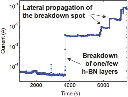
Multilayer hexagonal boron nitride (h‐BN) is an insulating 2D material that shows good interaction with graphene and MoS2, and it is considered a very promising dielectric for future 2D‐materials‐based electronic devices. Previous studies analyzed the dielectric properties of thick (>10 nm) mechanically exfoliated h‐BN nanoflakes (diameter < 20 μm) via conductive atomic force microscopy and applying very high voltages (>10 V); however, these methods are not scalable. In this work, the first device‐level reliability study of large area h‐BN dielectric stacks (grown via chemical vapor deposition) is presented, and the complete dielectric breakdown (BD) process is described. The experiments and calculations indicate that the BD process in metal/h‐BN/metal devices starts with a progressive current increase across the h‐BN stack until current densities up to 0.1 A cm−2 are reached. After that, the currents increase by sudden steps, which can be large (>1 order of magnitude, related to the BD of one/few h‐BN layers) or small (<1 order of magnitude, related to the lateral propagation of the BD). The bimodal BD process of h‐BN here presented (which cannot be detected via conductive atomic force microscopy) is essential to understand the reliability of 2D‐material‐based electronic devices using h‐BN as dielectric.
中文翻译:

使用化学气相沉积六方氮化硼作为介电体的电子器件中的双峰介电击穿
多层六方氮化硼(h-BN)是一种绝缘2D材料,与石墨烯和MoS 2表现出良好的相互作用,并且它被认为是未来基于2D材料的电子设备的非常有希望的电介质。先前的研究通过导电原子力显微镜和施加非常高的电压(> 10 V)来分析厚(> 10 nm)的机械剥落的h-BN纳米薄片(直径<20μm)的介电性能;但是,这些方法不可扩展。在这项工作中,提出了大面积h-BN电介质堆叠(通过化学气相沉积生长)的设备级可靠性研究,并描述了完整的电介质击穿(BD)过程。实验和计算表明,金属/ h-BN /金属器件中的BD过程始于整个h-BN堆的电流逐渐增加,直到电流密度高达0.1 A cm -2为止达到。此后,电流突然增加,可能大(> 1个数量级,与一个/几个h-BN层的BD有关)或小(<1个数量级,与该层的横向传播有关)。 BD)。此处介绍的h-BN的双峰BD过程(无法通过导电原子力显微镜检测到)对于了解使用h-BN作为电介质的基于2D材料的电子设备的可靠性至关重要。
更新日期:2018-01-15
中文翻译:
使用化学气相沉积六方氮化硼作为介电体的电子器件中的双峰介电击穿
多层六方氮化硼(h-BN)是一种绝缘2D材料,与石墨烯和MoS 2表现出良好的相互作用,并且它被认为是未来基于2D材料的电子设备的非常有希望的电介质。先前的研究通过导电原子力显微镜和施加非常高的电压(> 10 V)来分析厚(> 10 nm)的机械剥落的h-BN纳米薄片(直径<20μm)的介电性能;但是,这些方法不可扩展。在这项工作中,提出了大面积h-BN电介质堆叠(通过化学气相沉积生长)的设备级可靠性研究,并描述了完整的电介质击穿(BD)过程。实验和计算表明,金属/ h-BN /金属器件中的BD过程始于整个h-BN堆的电流逐渐增加,直到电流密度高达0.1 A cm -2为止达到。此后,电流突然增加,可能大(> 1个数量级,与一个/几个h-BN层的BD有关)或小(<1个数量级,与该层的横向传播有关)。 BD)。此处介绍的h-BN的双峰BD过程(无法通过导电原子力显微镜检测到)对于了解使用h-BN作为电介质的基于2D材料的电子设备的可靠性至关重要。


 京公网安备 11010802027423号