当前位置:
X-MOL 学术
›
Adv. Opt. Mater.
›
论文详情
Our official English website, www.x-mol.net, welcomes your
feedback! (Note: you will need to create a separate account there.)
Flat Optical and Plasmonic Devices Using Area‐Selective Ion‐Beam Doping of Silicon
Advanced Optical Materials ( IF 8.0 ) Pub Date : 2018-01-15 , DOI: 10.1002/adom.201701027 Jad Salman 1 , Martin Hafermann 2 , Jura Rensberg 2 , Chenghao Wan 1, 3 , Raymond Wambold 1 , Bradley S. Gundlach 1 , Carsten Ronning 2 , Mikhail A. Kats 1, 3
Advanced Optical Materials ( IF 8.0 ) Pub Date : 2018-01-15 , DOI: 10.1002/adom.201701027 Jad Salman 1 , Martin Hafermann 2 , Jura Rensberg 2 , Chenghao Wan 1, 3 , Raymond Wambold 1 , Bradley S. Gundlach 1 , Carsten Ronning 2 , Mikhail A. Kats 1, 3
Affiliation
|
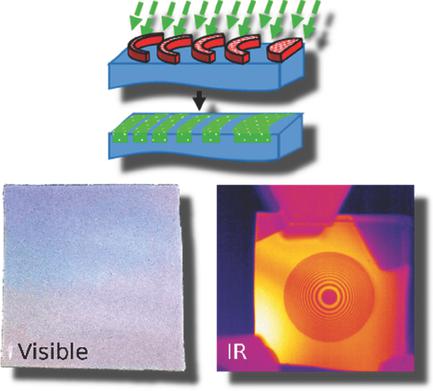
Highly doped semiconductors are an emerging platform for plasmonic devices. Unlike in noble metals, the carrier concentration of semiconductors can vary by many orders of magnitude, resulting in a widely tunable range of plasma wavelengths spanning the mid‐infrared and terahertz ranges. In this work, the potential of highly doped, ion‐beam‐patterned silicon is demonstrated as a fabrication‐friendly platform for flat optical devices. Detailed characterization of the optical properties of silicon is performed at various doping levels, and diffractive optical elements and plasmonic frequency‐selective surfaces that operate in the mid‐to‐far‐infrared regime are realized. The resulting optical devices are monolithic, flat, resilient to thermal and physical damage, and can be easily integrated into other silicon‐based platforms.
中文翻译:

使用硅的区域选择性离子束掺杂的平面光学和等离子设备
高掺杂半导体是等离子体设备的新兴平台。与贵金属不同,半导体的载流子浓度可以变化多个数量级,从而导致等离子波长的可调节范围跨越中红外和太赫兹范围。在这项工作中,高掺杂的离子束图案化硅的潜力被证明是用于平面光学设备的易于制造的平台。在不同的掺杂水平上对硅的光学性质进行了详细的表征,并实现了在中红外范围内工作的衍射光学元件和等离激元频率选择表面。最终的光学器件是整体的,扁平的,对热和物理损坏具有弹性的器件,并且可以轻松集成到其他基于硅的平台中。
更新日期:2018-01-15
中文翻译:
使用硅的区域选择性离子束掺杂的平面光学和等离子设备
高掺杂半导体是等离子体设备的新兴平台。与贵金属不同,半导体的载流子浓度可以变化多个数量级,从而导致等离子波长的可调节范围跨越中红外和太赫兹范围。在这项工作中,高掺杂的离子束图案化硅的潜力被证明是用于平面光学设备的易于制造的平台。在不同的掺杂水平上对硅的光学性质进行了详细的表征,并实现了在中红外范围内工作的衍射光学元件和等离激元频率选择表面。最终的光学器件是整体的,扁平的,对热和物理损坏具有弹性的器件,并且可以轻松集成到其他基于硅的平台中。


 京公网安备 11010802027423号