当前位置:
X-MOL 学术
›
Adv. Opt. Mater.
›
论文详情
Our official English website, www.x-mol.net, welcomes your
feedback! (Note: you will need to create a separate account there.)
Enhanced Light Extraction from OLEDs Fabricated on Patterned Plastic Substrates
Advanced Optical Materials ( IF 8.0 ) Pub Date : 2018-01-04 , DOI: 10.1002/adom.201701244 Chamika Hippola 1, 2 , Rajiv Kaudal 1, 2 , Eeshita Manna 3 , Teng Xiao 1, 2 , Akshit Peer 1, 3, 4 , Rana Biswas 1, 2, 3, 4 , Warren Dennis Slafer 5 , Tom Trovato 6 , Joseph Shinar 1, 2 , Ruth Shinar 3, 4
Advanced Optical Materials ( IF 8.0 ) Pub Date : 2018-01-04 , DOI: 10.1002/adom.201701244 Chamika Hippola 1, 2 , Rajiv Kaudal 1, 2 , Eeshita Manna 3 , Teng Xiao 1, 2 , Akshit Peer 1, 3, 4 , Rana Biswas 1, 2, 3, 4 , Warren Dennis Slafer 5 , Tom Trovato 6 , Joseph Shinar 1, 2 , Ruth Shinar 3, 4
Affiliation
|
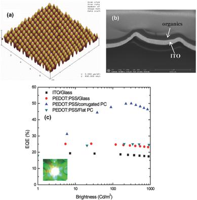
A key scientific and technological challenge in organic light‐emitting diodes (OLEDs) is enhancing the light outcoupling factor ηout, which is typically <20%. This paper reports experimental and modeling results of a promising approach to strongly increase ηout by fabricating OLEDs on novel flexible nanopatterned substrates that result in a >2× enhancement in green phosphorescent OLEDs (PhOLEDs) fabricated on corrugated polycarbonate (PC). The external quantum efficiency (EQE) reaches 50% (meaning ηout ≥50%); it increases 2.6x relative to a glass/ITO device and 2× relative to devices on glass/poly(3,4‐ethylenedioxythiophene):polystyrene sulfonate (PEDOT:PSS) or flat PC/PEDOT:PSS. A significant enhancement is also observed for blue PhOLEDs with EQE 1.7× relative to flat PC. The corrugated PC substrates are fabricated efficiently and cost‐effectively by direct room‐temperature molding. These substrates successfully reduce photon losses due to trapping/waveguiding in the organic+anode layers and possibly substrate, and losses to plasmons at the metal cathode. Focused ion beam gauged the conformality of the OLEDs. Dome‐shaped convex nanopatterns with height of ∼280–400 nm and pitch ∼750–800 nm were found to be optimal. Substrate design and layer thickness simulations, reported first for patterned devices, agree with the experimental results that present a promising method to mitigate photon loss paths in OLEDs.
中文翻译:

从图案化塑料基板上制造的OLED增强光提取
在有机发光二极管(OLED)的一个关键的科学和技术挑战是提高光输出耦合系数η出,其通常<20%。本文报道有前途的方法的实验和模拟结果强烈增加η出通过在新颖的柔性纳米图案衬底上制造的OLED的是结果在> 2×增强在绿色磷光OLED(PHOLED中)上的波纹聚碳酸酯(PC)制成。外部量子效率(EQE)达到50%(意思是η出≥50%); 相对于玻璃/ ITO设备,它增加了2.6倍,而相对于玻璃/聚(3,4-乙烯二氧噻吩):聚苯乙烯磺酸盐(PEDOT:PSS)或平板PC / PEDOT:PSS上的设备,它增加了2倍。与平板PC相比,具有EQE 1.7倍的蓝色PhOLED还可观察到显着增强。瓦楞纸基板可以通过直接室温模制来高效,经济地制造。这些基板成功地减少了由于有机+阳极层(可能还有基板)中的俘获/波导而造成的光子损失,以及金属阴极上的等离激元的损失。聚焦离子束测量了OLED的保形性。发现高度约为280-400 nm,节距约为750-800 nm的圆顶形凸纳米图案是最佳的。基板设计和层厚度模拟,首先报道了有图案的器件,
更新日期:2018-01-04
中文翻译:
从图案化塑料基板上制造的OLED增强光提取
在有机发光二极管(OLED)的一个关键的科学和技术挑战是提高光输出耦合系数η出,其通常<20%。本文报道有前途的方法的实验和模拟结果强烈增加η出通过在新颖的柔性纳米图案衬底上制造的OLED的是结果在> 2×增强在绿色磷光OLED(PHOLED中)上的波纹聚碳酸酯(PC)制成。外部量子效率(EQE)达到50%(意思是η出≥50%); 相对于玻璃/ ITO设备,它增加了2.6倍,而相对于玻璃/聚(3,4-乙烯二氧噻吩):聚苯乙烯磺酸盐(PEDOT:PSS)或平板PC / PEDOT:PSS上的设备,它增加了2倍。与平板PC相比,具有EQE 1.7倍的蓝色PhOLED还可观察到显着增强。瓦楞纸基板可以通过直接室温模制来高效,经济地制造。这些基板成功地减少了由于有机+阳极层(可能还有基板)中的俘获/波导而造成的光子损失,以及金属阴极上的等离激元的损失。聚焦离子束测量了OLED的保形性。发现高度约为280-400 nm,节距约为750-800 nm的圆顶形凸纳米图案是最佳的。基板设计和层厚度模拟,首先报道了有图案的器件,


 京公网安备 11010802027423号